

Substrate
X-ray lithography worked. The industry chose a different path. Substrate wants to go back. Will it work? What about XLight, ASML, TSMC?

Today, we’re talking Substrate.
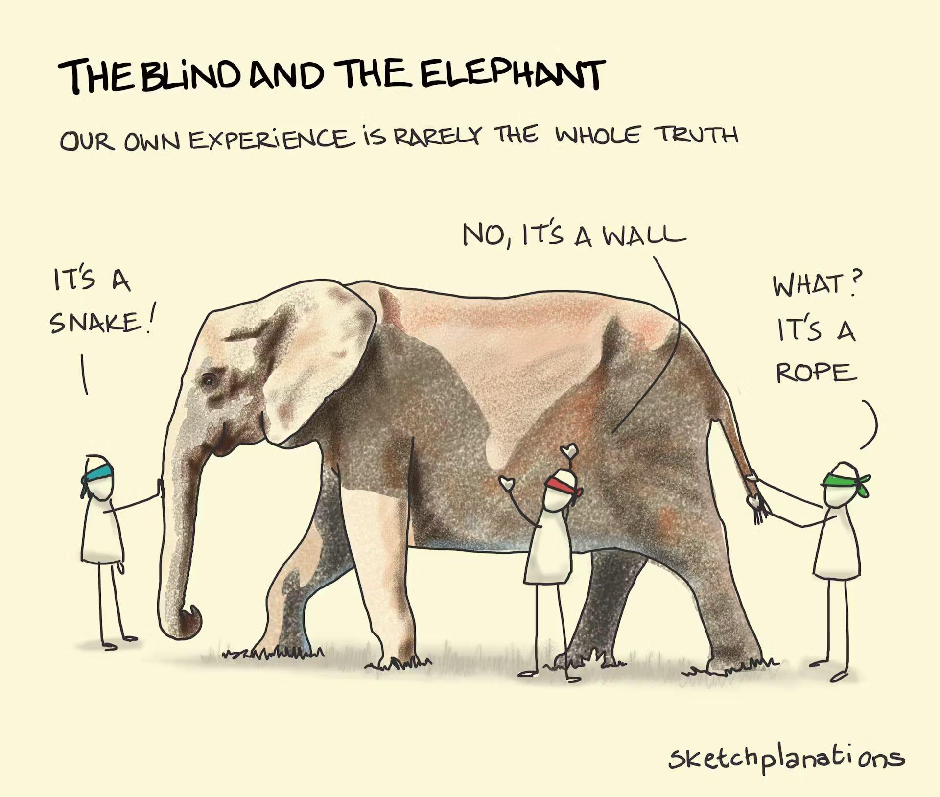
Substrate is controversial. The debate tends to focus on individual objections, such as a lack of industry experience or the impracticality of particle accelerators. But I want to zoom out and look at the elephant as a whole:
To do that, let’s use a simple framework to test whether Substrate’s strategy is actually sound.
How to Solve Problems
A while back, I was listening to an old Lex Fridman podcast with Ray Dalio. And Ray was talking about his “5-Step Process”:
Set your goal
Identify the problems blocking it
Diagnose the root cause
Design around it
Follow through
Not rocket science. But there’s power in simple frameworks as a lens to view the world.
These five steps resonated with me, as they pattern-match well with my lived experiences (entrepreneurship, engineering, academic research, home projects, and so on). Once I heard it, I started seeing it everywhere. Listening through the How I Built This backlog, I found it in the Crate & Barrel founding story from the 1960s. Let me show you how it applies there, and then we’ll try it on Substrate.
Crate & Barrel
Quick context: Summer 1961. Gordon and Carol Segal are getting married. Both 23. They registered for stylish European housewares, but nobody in their lives had the money or taste to buy it for them. The Segals couldn’t afford it either.
But on their honeymoon in the Caribbean, they found the same products at a fraction of US prices:
Gordon Segal: There was one Scandinavian store in the Virgin Islands. My wife picked up some of the items and said, “How can you have Danish 18/8 stainless at the $2.95 a place setting? It’s so much more expensive in America!”
And the Danish merchant there said, “We have salesmen from Europe come here, and we buy direct from factories.”
Ah! A goal, a problem, a root cause. Gordon’s wheels started spinning:
We got back to Chicago, and I was in the real estate business. She was teaching school. We were both sort of bored. And then, one night in February of ‘62, I was washing these dishes we had bought. I said, “You know, Carol, there had to be other young people like ourselves with good taste and no money. We should open a store.”
Through the Dalio lens (and listening to the rest of the podcast):
Goal: Sell beautiful European housewares to young people with good taste and no money.
Problem: Those goods were priced out of reach in the US, even though they were affordable in Europe and the Caribbean.
Root cause: Middlemen in the US import distribution chain.
Design: Skip the importers. Buy direct from European factories.
Follow through: Hard work and grit.
The Segals didn’t pencil out this strategy cleanly from Day 1. But the Dalio process was at work.
Now let’s apply it to Substrate.
Substrate
Substrate CEO James Proud made the goal very clear in this Stratechery interview: revive American chip manufacturing leadership.
WTF? REVIVE AMERICAN CHIP MANUFACTURING? WHO DOES HE THINK HE IS?
Before you grab pitchforks, let’s work through the reasoning. We’ll address “yeah but no industry experience” and the rest later. First, the 5-step process.
Goal: American leading-edge semiconductor manufacturing
What obstacles stand in the way?
Money and talent come to mind first. But those aren’t fundamental bottlenecks. Think about Elon and Terafab. Money and talent are tractable.
Dig deeper. Assume you’re well-capitalized and talent-rich. OK, this sounds like Rapidus. We can cover them in another article.
Now what?
You know what’s actually hard? Creating a customer.
Problem: No one will work with you
Customer acquisition is the problem.
How could you possibly incentivize chip designers to use a brand-new, leading-edge foundry? You need a reason so compelling that it overcomes the risk premium.
On what plane can you even outperform TSMC?! They have 30+ years of process knowledge and relationships with every major chip company on Earth. And don’t say supply chain security. TSMC has n-1 capacity in Arizona and Intel Foundry is getting its swagger back…
Hmm…
Well, what pain points do chip designers have with TSMC today?
Cost is a big one.
The Cost Problem
Many companies can’t afford leading-edge nodes, and even those that can only use them for a select few SKUs. Design costs run in the hundreds of millions. Mask sets cost tens of millions. Only products with massive volume (smartphones) or high ASPs (Nvidia GPUs) can amortize that cost. And variable costs compound it. Leading-edge wafers are north of $20K and all signs point toward $100K by the end of the decade. So even for the highest-volume products, where fixed costs amortize to near zero, wafer price still matters.
Why is the leading edge so expensive? Lithography.
EUV tools cost hundreds of millions each and the cost is only going up. You need dozens per fab, a significant driver of leading edge fab requires tens of billions to build. Deeper background reading here:

But… what if you could somehow reduce the cost of lithography drastically?
What if you could offer a value proposition of “2nm wafers at 28nm prices”?
You could create customers. Existing medium and low volume SKUs that would love to use smaller, more power efficient transistors or build their own custom ASICs instead of using less efficient/broader off-the-shelf options.
Yeah, but EUV LITHOGRAPHY IS MAGIC! TIN DROPLETS! 30+ YEARS! ASML! NO WAY!
Yes, I know. Suspend disbelief for a bit and just follow Dalio’s process. Let’s pull on the thread more.
What is the root cause of the lithography economics problem?
XLight has rightly pointed out that Laser-Produced Plasma (LPP) is very expensive. The “shoot tin droplets and hit them twice with a laser to generate EUV light” part. And every ASML EUV machine needs one.
XLight says, “Why not use a much higher power free electron laser (FEL) and share that light source amongst many EUV scanners?” This unlocks much better economics, not only from decoupling the light source from the scanner but also by increase the dose which impacts productivity and wafer economics.
See more here:

But what if you pull on the root cause even further? Could it lead to a different solution?
The entire EUV system (light source, optics, scanner) is incredibly complex with known inefficiencies (many mirrors, lots of lost light…) all driving extreme cost.
Is that cost due to physics, meaning this is the globally optimal solution, and there is a physical limit preventing lithography from ever working differently?
Or did path dependence lead us to a local minimum, not a global one?
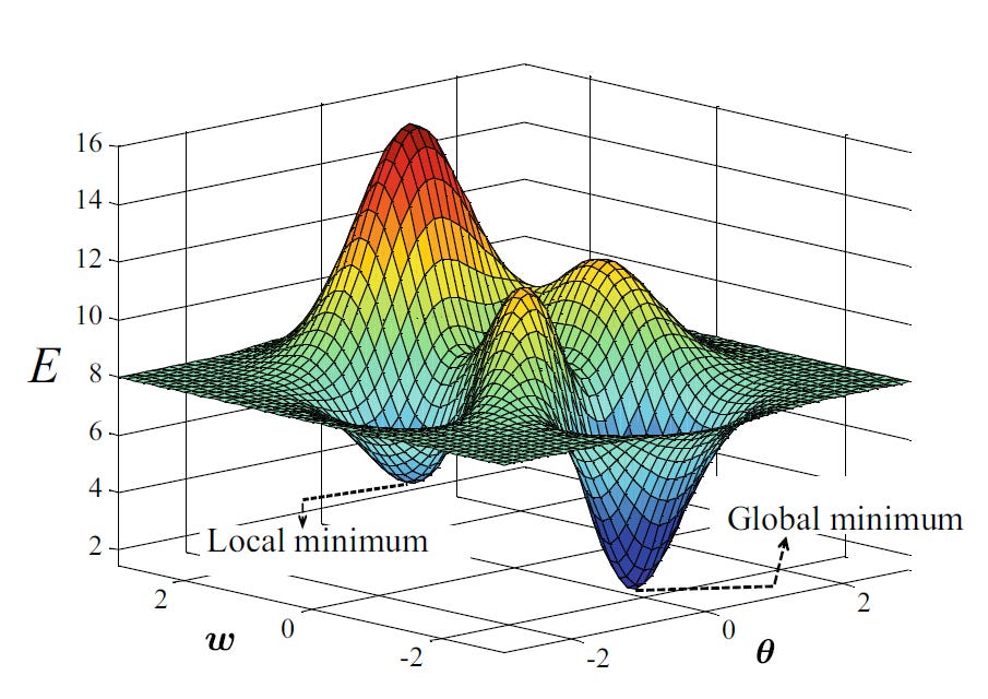
Is the root cause physics, or path dependence?
Retracing The Path
Substrate believes it’s path dependence. And you can actually retrace the history to test that claim. In the ‘80s and ‘90s, the industry was actively researching X-ray lithography, which has a natural resolution advantage from its shorter wavelength.
Hmm… maybe we could learn what the shortcomings were and if they are till true today!
There are great old papers on this, especially from IBM Research. Check out this paper “X-ray lithography in IBM, 1980-1992, the development years”. It’s super enlightening. Let’s keep pulling on the thread, from Alan D. Wilson’s paper:
Optical lithography, in 1980, was very poorly understood by the experts. On the basis of historical trends and current difficulties with existing tooling and technology, the limits of lithography were thought to be about 1–1.25 µm for optics. X-ray lithography, consequently, was targeted for entry around 1 µm, the perceived limit of optical lithography.
At the onset of the program the strategic advantages of X-ray lithography were stated to be high resolution (better than optical lithography), throughput superior to that of e-beam technology, better resist-processing characteristics, and potentially lower defects (no multilayer resists).
X-ray seemed promising at the time. What did they learn? How did they learn? Were they thinking about manufacturability or just science?
We spent the remainder of 1980 developing a financial and technical program plan for X-ray lithography based on synchrotrons, considering a number of basic questions: Where were exposures going to be done? What should the mask be made from, and how would it look? How would we develop a stepper/aligner system, and what would be the role of vendor assistance in this regard? What would be the staffing needs (the initial group included only six people) as the program progressed? And finally, what should the test vehicle be?
It was recognized early in the drafting of our program that we were targeting manufacturing, not device prototyping, but full manufacturing. Our manufacturing divisions would eventually be our customer.
That’s really sound and reasonable thinking. They were thinking about full production scale and manufacturability, not just the science. And if you read the rest of the paper, the X-ray lithography (XRL) technology actually worked:
We had made complex, fully scaled CMOS devices with 0.5-μm ground rules before our optical counterparts had reached the same level using a long-established technology. Our yield was also acceptable: not 100%, but acceptable. The principal goal of the X-ray program had been achieved.
There are even tips for Substrate and us to think consider regarding a practical particle accelerator:
For X-ray lithography to be viable in IBM, we needed to explore acquiring our own X-ray source… Early in 1982, Grobman and I were starting to learn about the physics of synchrotrons. Our interest in a synchrotron ring for IBM was kindled by reports from Munich of the design of a tabletop machine called Kleine-Erna…. We began this serious inquiry by visits to established rings in this country and in Europe. Perhaps not being part of the synchrotron establishment was beneficial: We could ask questions and find out what really made rings good and what did not, as well as who the real experts were.
A quick aside… Agree. Perhaps not being part of the establishment is a benefit at times. … And figure out who the *real* experts are 😂
This IBM researcher Alan D. Wilson is my dude.
Anyway, he continues
Armed with this information, we asked ourselves what the specifications for the ring should be… I was invariably asked “What should a ring for industry be?” My answer was this: It should fit on a truck; plug into a wall socket; be reliable and available to operate 20 out of 21 shifts per week; have sufficient average output capable of sustaining a stepper throughput of more than 30 wafers per hour using an insensitive (having a sensitivity of -100 mJ/cm^) X-ray resist; be capable of being debugged/commissioned and assembled at the vendor, shipped intact to an IBM site, and rendered operational in a reasonable time at full specifications.
Make sure it fits on a truck and plugs into a wall socket. Quite practical!
And that kind of thinking is a lot different than the picture of particle accelerators I had in my head (i.e. CERN).
Oh last quick note from the paper, it seems that folks exploring XRL have always been doubted.
The establishment of a program was a formidable task, since half of this distinguished group seriously questioned the need for and the viability of X-ray lithography.
But IBM actually built a synchrotron (“Helios”) that fit on a truck and worked:
Oxford proposed a superconducting dipole system with a cold bore. The magnet turned out to be difiicult to construct but had excellent performance. The Helios 1 ring was completed and commissioned at Oxford, England, in October 1990. During the design and building of the synchrotron we visited Oxford and the Daresbury team every four to eight weeks over a period of three and a half years. The ring was shipped to IBM in March 1991 and arrived at East Fishkill on March 29, 1991. It fit on a truck, as shown in Figure 12(a), and we slid it into ALF that same day [Figure 12(b)].
The first beam was stored on or about May 20, 1991, and final specifications were met in January 1992. Our goal had been met and, in fact, exceeded, because the ring performs beyond specification [36]. Critics who thought design alone would not work were wrong. IBM and Oxford as a development team commissioned the Oxford ring in record time and with a very high level of performance.
If it worked back then… why don’t we have X-ray lithography today? XRL wasn’t without practical shortcomings at the time. This IBM paper from 1998 said that XRL was mature enough to possibly be introduced at 130nm node, but admitted manufacturing issues, for example with masks.
Nonetheless, there are challenges still to be met. Among the most important are the development and commercial availability of an improved e-beam mask writer; the ability to fabricate defect-free masks satisfying the image placement and critical dimension control requirements with good yields; the stability of the masks in usage (including the issue of possible radiation damage); the ability to correct for magnification errors; and the ability to satisfy the industry’s desire for a technology extendible to 70 nm ground rules. These issues are primarily manufacturing issues, as opposed to issues related to demonstrating proof-of-concept or feasibility, although demonstrating extendibility is still needed before the industry can commit to using XRL at 70 nm ground rules
XRL was physically feasible but had engineering problems to solve at production scale.
Meanwhile, optical lithography kept working far beyond the ~1μm wall Wilson predicted. So the industry kept pushing optical. First DUV, then EUV.
But a lot has changed in 35 years. US National Labs have spent years advancing particle accelerators and sources are now brighter, more reliable, and more compact. Computational lithography has improved significantly, too, and can help overcome the mask and proximity challenges that plagued IBM.
Substrate’s Design
So back to the Dallio process. The bottleneck is EUV-based lithography economics, and Substrate’s approach is to go back to the fork in the road and choose a different path. Could there be a global optimum, and could it be XRL?
It would require co-designing the light source, optics, and scanner as an integrated whole from scratch. But to me, there seem to be many cost savings possibilities on the table:
One particle accelerator source feeds many scanners, like IBM’s Helios ring which had 16 beamline ports. The light source cost amortizes across many tools.
No multilayer mirrors means no compounding reflectivity losses. Almost all generated photons are available at the wafer, vs. single-digit percent for EUV.
No tin-droplet plasma source means no tin contamination, no collector degradation, no droplet generator maintenance.
Single-patterning at leading-edge nodes. Fewer exposures = fewer masks, fewer etch steps, fewer defect opportunities, faster cycle time.
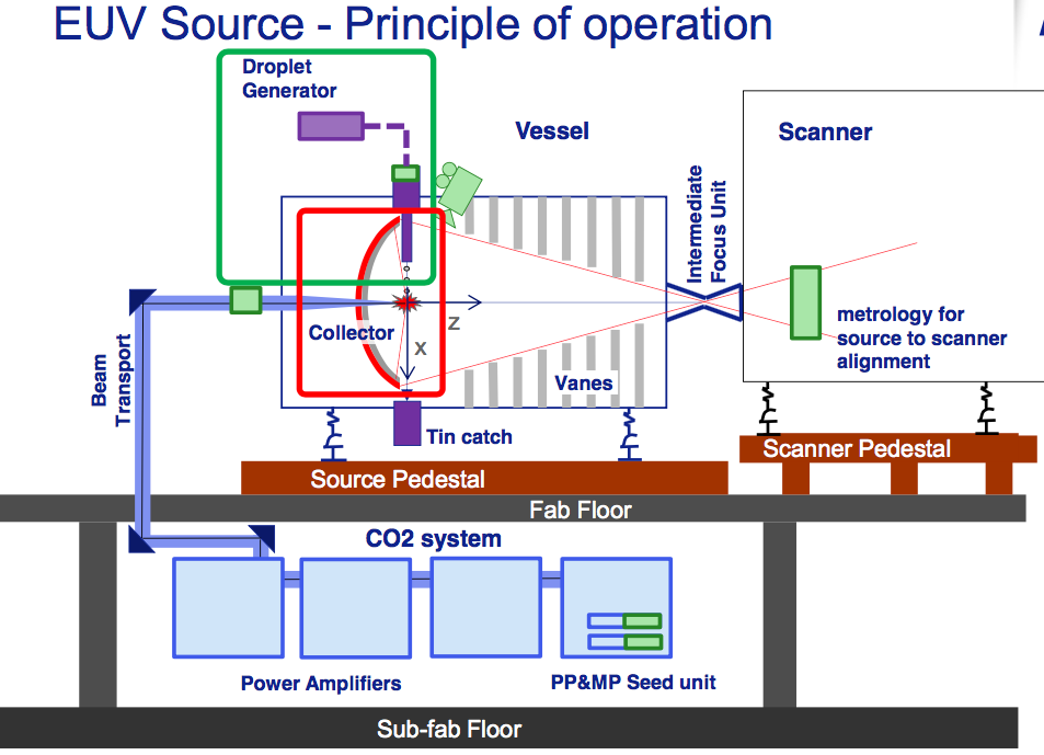
In theory, the particle accelerator shouldn’t need cleanroom space. Only the wafer-handling end of the beamline sits in the cleanroom. This is contrary to EUV scanners which are massive and require substantial fab and subfab infrastructure:
So here’s the chain of reasoning so far:
Goal: American leading-edge semiconductor manufacturing
Problem: No one will work with a new foundry
Root cause: The only lever that overcomes the risk premium is dramatically lower cost, and cost is dominated by lithography
Root cause (a layer deeper): EUV’s cost comes from path dependence, not physics
Design: Go back to the 1990 fork. X-ray lithography with modern sources.
This is sound. It sure seems XRL could genuinely untangle the lithography cost problem.
It’s believable. And it’s fundable. Substrate raised $100M from Founders Fund, General Catalysts, In-Q-Tel, and more. Founder’s Fund’s thesis is to invest in smart people solving difficult scientific problems where, if they succeed, the technology would be extraordinarily valuable. Substrate is a perfect fit. A 1% chance of reshaping the $1T+ semiconductor industry seems like just the type of asymmetric bet FF was built to make.
Of course, sound strategy doesn’t guarantee success. Execution is everything.
So can they actually pull this off? Behind the paywall I address the biggest objections head-on, work through whether XLight and Substrate can both win, and discuss the impact to TSMC and ASML.
It’s really, really interesting.