

xLight. Photons as a Service.
xLight's plan to swap EUV's light source for a free-electron laser and sell light like a utility.

In January, I wrote about the worsening cost curve of EUV lithography and two startups trying to bend it:

I teased xLight and Substrate and promised deeper dives on both.
Today I’m delivering the first one on xLight. Now that we understand the broader economic problem the industry needs to solve, let’s dive into technical details and areas for improvement.
We’ll start with some fundamental limits of LPP EUV scanners.
The Photon Problem
Every ASML EUV scanner generates its light the same way. It’s called Laser Produced Plasma, or LPP. It’s the “shoot tin droplets and hit ‘em each twice with a laser” light source magic trick. I’m assuming most readers are somewhat familiar, but if not here are great YouTubes references get you up to speed plus a short recap
How EUV’s light source LPP works: A high-intensity CO2 laser fires at tiny droplets of molten tin traveling at 100 meters per second, 50,000 times per second. Each droplet is actually hit twice: first a pre-pulse reshapes the 30-micrometer tin sphere into a concave sheet, then the main CO2 pulse vaporizes it into a dense plasma that emits 13.5nm EUV photons. These photons bounce off a series of collector mirrors, pass through a photomask, and expose the wafer below. As you can imagine, it took decades to get this concept to work at reliability and yield needed for scaled manufacturing. It’s freaking nuts that it works. That’s what I love about the semiconductor industry by the way, literally everywhere you look it’s just mind-blowing technology.
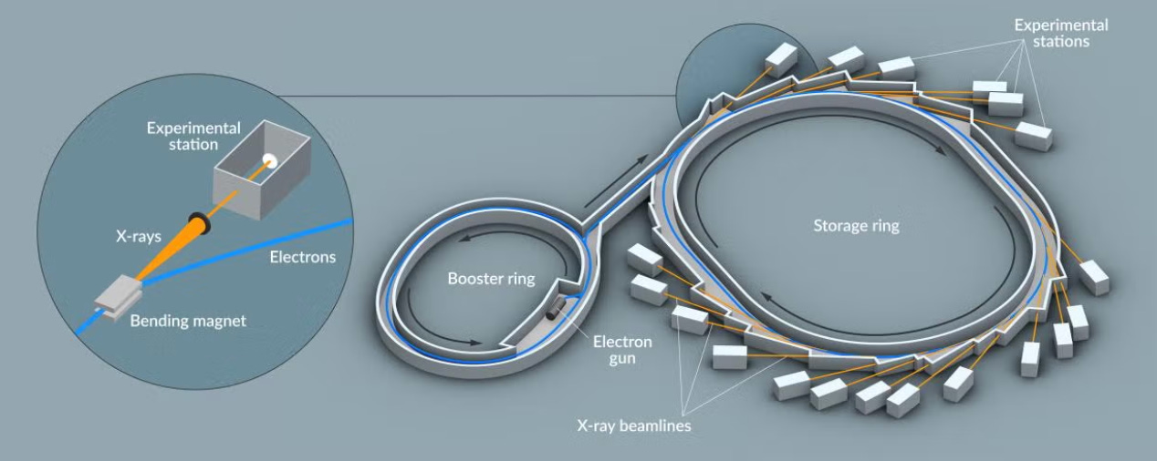
One interesting thing to note is that the industry actually first tried particle accelerators called synchrotrons to generate this high-energy, small-wavelength light. But at the time, synchrotrons didn’t have enough directional light. Next they tried xenon gas lasers, but that had a fundamental physics ceiling resulting in less than 1% conversion efficiency. Eventually the industry landed on tin back in 2002. Blasting tin particles into a plasma produces EUV light, but it has a debris problem (contaminating everything). That’s an engineering problem though (how to deal with this debris) but not a fundamental physics roadblock.
Fast forward 20 years and LPP with tin works. Hitting 50,000 falling tin droplets per second with a laser, twice each, 24/7. It’s genuinely an engineering marvel, should be discussed in freshman physics and engineering classes to get people excited about science
But.... the best LPP achieves only about 6% conversion efficiency. 94% of the energy put in is wasted. And the system has fundamental problems that get worse as chips get smaller.
For example, EUV photons carry about 14x more energy than the 193nm photons used in previous-generation DUV lithography. That means for the same power output, an EUV source produces 14x fewer photons.
This is where dose comes in. Dose is the amount of light energy delivered per unit area of the wafer, measured in millijoules per square centimeter (mJ/cm²). Think of it as the photon budget for each exposure. The photoresist (the light-sensitive chemical coating on the wafer) needs a minimum number of photons to trigger the chemical reaction that creates the pattern. Too few photons and edges come out rough or some features are missing:
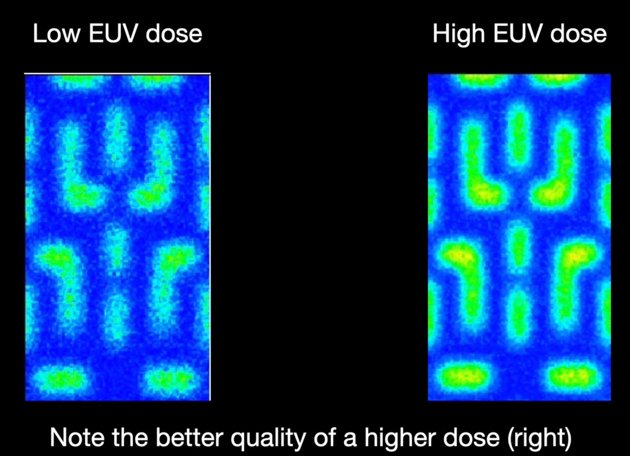
The required dose isn’t a knob you can turn down to save time, as it’s set by the resist chemistry and the feature size. And as features shrink, dose requirements go up. Why? Because smaller features mean each “pixel” on the wafer covers fewer atoms of resist. Fewer atoms mean fewer photon interactions, leading to greater statistical randomness in whether the pattern prints correctly. To compensate, you need more photons per pixel (a higher dose) to keep the randomness under control. The industry calls these randomness problems stochastic effects, and as Asianometry puts it:
“Stochastic print failures are far smaller, completely random and thus non-repeating, and come via a law of nature. The randomness is unavoidable. So how do we usually deal with randomness caused by the law of small numbers? We increase numbers. Just send more photons.”
So every new node needs a higher dose, but the light source isn’t getting proportionally brighter.
For example, a Low-NA EUV tool is rated for about 220 wafers per hour:
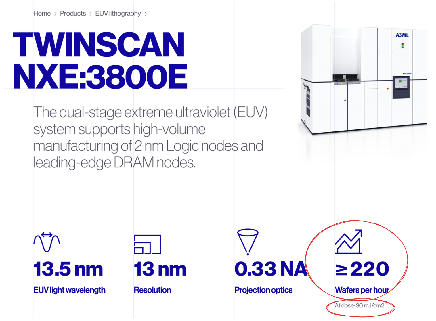
But that rating assumes a dose of 30 mJ/cm². Move to High-NA which prints finer features and needs a higher dose and look what happens:
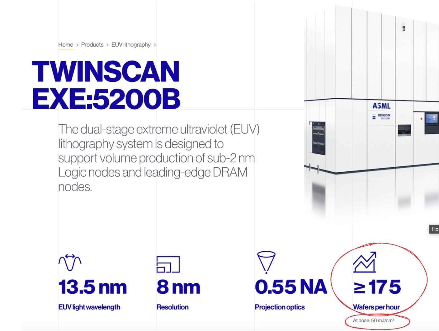
Notice throughput is only 175 wafers per hour at 50 mJ/cm².
The more advanced tool is slower because the higher dose eats into throughput. High-NA can save you total exposure steps by eliminating double patterning, which helps. But the long-term trend is evident. Every step to smaller features demands more dose, and more dose means fewer wafers per hour unless the light source gets brighter. Today’s LPP sources produce about 500 watts of EUV power. ASML has shown a roadmap to 600-800 watts. Note: per this week’s ASML disclosure in Reuters, ASML says its R&D team has unlocked 1,000+ W which would increase throughput back up to >300 wph.
But it’s still not enough. Why not? Because dose requirements are increasing too. Low-NA needs 30 mJ/cm² and High-NA needs 50+ mJ/cm². Future nodes will push higher as stochastic effects worsen with each shrink.
And that’s just the power problem. Most of the photons you do generate never reach the wafer. Tin debris fogs the collector mirrors. A layer just 1.2nm thick cuts collector efficiency by 20%. And each mirror in the optical chain absorbs about 30% of the light that hits it, so after the full series of reflections, less than 10% of source photons make it to the wafer.
Then the kicker. Every scanner has its own dedicated LPP source. A fab running 15 EUV tools is operating 15 separate tin-burning light sources, each 6% efficient, each losing 90%+ to mirrors, each fighting its own debris.
Whew. Again, it’s a miracle it even works. But it’s pretty inefficient, and the problems mount as we look ahead on the EUV roadmap.
With LPP light sources, lithography costs will continue to increase. It’s inevitable. And as we discussed in the first article in this series, those costs have a real impact on the broader industry.
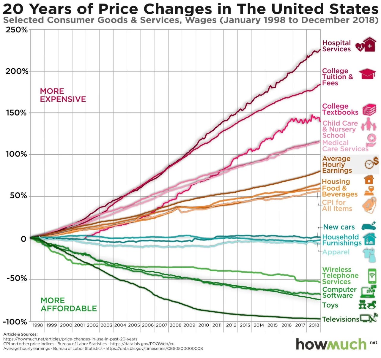
Kind of reminds me of this chart... we need to bend the cost per chip of lithography downward over time...like good technology curves do…
A Different Way to Make Light
But what if there were a light source that produced orders of magnitude more power, eliminated tin entirely, and could serve an entire fleet of scanners from a single system?
That’s a Free Electron Laser.
(Shout out Asianometry again! A great video on the topic if you want the deep dive.)
Remember that the industry first tried synchrotrons for EUV back in the 1980s, but rejected them because the light was too diffuse.
A Free Electron Laser is different. Instead of passively emitting radiation as electrons circle, an FEL actively amplifies coherent, directional light through a linear accelerator. Directional light! That distinction solves the problem that killed synchrotrons.
Here’s the short version of how an FEL works. A linear accelerator shoots electrons to near light speed, then sends them through an undulator, a chain of alternating magnets that wiggles the beam back and forth. That wiggling causes the electrons to emit photons, which interact with the beam itself, causing the electrons to self-organize into coherent bunches that amplify the light exponentially. The result is intense, coherent, laser-like light:
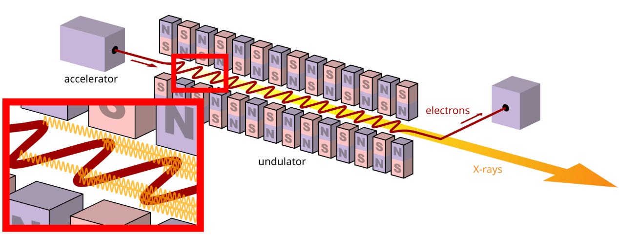
Exactly what EUV scanners need! No tin. No plasma. No debris. And you can tune it to 13.5nm to plug in this light source directly into existing 13.5nm EUV scanners!
Three properties make FELs really awesome for lithography.
Tunable wavelength. By adjusting the electron energy and magnet spacing, you can dial the output to any wavelength: 13.5nm for EUV, smaller for future “Beyond EUV” nodes, or even dial it back and use longer wavelengths for less cutting-edge process nodes.
Energy recovery. Instead of dumping spent electrons, you loop them back through the accelerator in reverse, recovering most of their kinetic energy. FEL light sources can be several times more efficient than LPP.
No tin, no debris. The entire contamination problem goes away. Cleaner light means longer mirror life and less maintenance downtime.
Enter xLight
xLight is a venture-backed company in Palo Alto building Free Electron Lasers purpose-built for semiconductor manufacturing. Their team comes from the US National Lab ecosystem, with deep experience designing, building, and operating FELs for research and national security. They’ve partnered with Fermilab on the superconducting cavity technology at the heart of the accelerator.
And they’re not doing this in a garage. Their prototype is being built at NY CREATES in Albany, NY, a semiconductor R&D hub where IBM runs a full 2nm process flow and where Tokyo Electron, Applied Materials, and other major equipment companies have a presence. xLight’s prototype was accelerated by investment from the Commerce Department as part of the CHIPS Act R&D program.
Replace the Source, Not the Scanner
So… what’s the product xLight sells? Well, light. xLight doesn’t compete with ASML’s scanners, but rather, replaces the light source. Unplug LPP, plug in xLight’s FEL.
xLight’s FEL is backward compatible with ASML’s existing scanner platforms. From the scanner’s perspective, the swap is transparent; the light comes in at the exact same angle, same wavelength, through the same intermediate focus point:
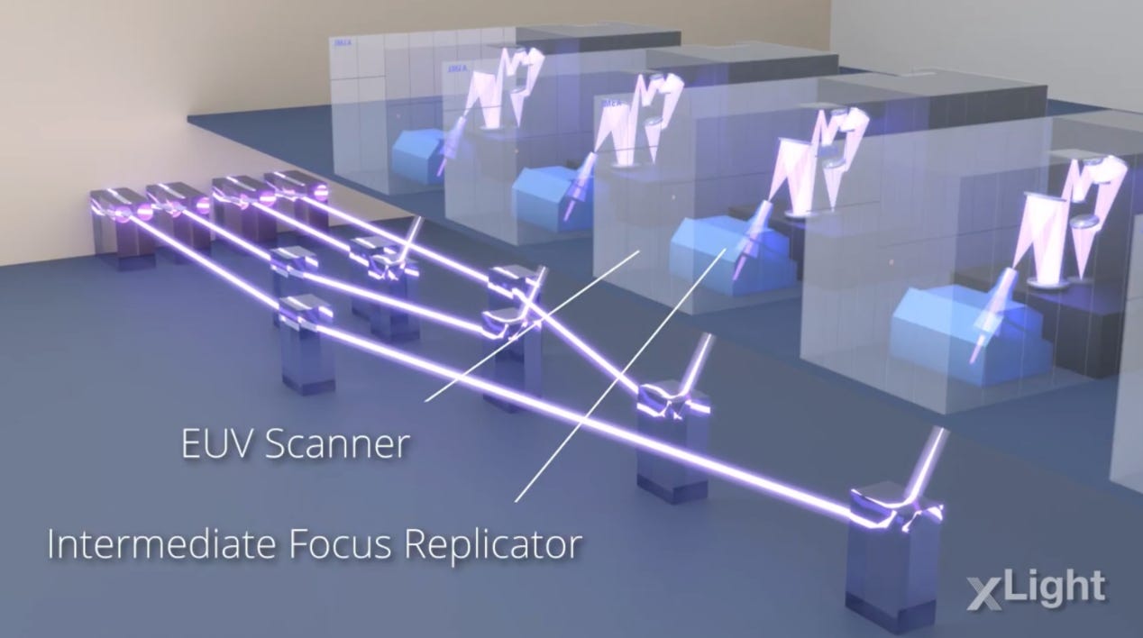
The only difference is that this approach doesn’t have tin splattering around and doesn’t have out-of-band radiation causing heat in the optics. In fact, because FEL light has a much narrower bandwidth than LPP, there’s less junk light and less thermal noise. Hence, the same scanner that’s designed for LPP light can actually handle more FEL light.
Oh, and did you notice in that image how many scanners are all being fed at the same time? This is the economic differentiator.
120 Kilowatts
xLight’s system generates 120 kilowatts of EUV power at the source.
Remember, current LPP sources produce just over 500 watts. ASML’s roadmap targets 800 watts. xLight is building a source that produces 120 kilowatts. Over 100x more power!
Now, you don’t get all 120 kW to the scanner. As light is distributed through the fab via vacuum beamlines and grazing-incidence optics, there are transmission losses. Depending on whether it’s a greenfield or brownfield fab, you deliver somewhere between 25% and 50% to the scanner fleet. Divided across up to say 16 scanner connections, that’s roughly 2-4 kilowatts per scanner. That’s still several times more than what LPP delivers today…
Abundant light unlocks the full dose at full productivity. No more running $500M High-NA tools at a slower speed because you can’t deliver enough photons. And beyond throughput, more light means better patterning. And that unlocks better uniformity and line edge roughness, resulting in higher yields. win win win.
xLight’s approach seems compelling. But there are still a lot of questions, like
How do they plan to sell it?
Who are the customers?
How to fund it? Building particle accelerators sounds expensive…
What does this mean for the broader lithography ecosystem?
Interestingly, if xLight’s economics work, it doesn’t necessarily disrupt ASML, and could arguably expand ASML’s addressable market. It’s nuanced though. We’ll get into it, as it has implications for anyone modeling ASML’s long-term revenue.
And the business model itself is fascinating. xLight doesn’t sell light sources. They sell light as a service, like a utility. Your electric bill is really just consumption-based electrons-as-a-service, right? We’ll dig into this.
And finally, adoption seems hard, right? I mean, semiconductor manufacturing is interestingly both super high-tech and yet quite conservative in some respects. Will they adopt?
Let’s get into it.