

Optics Primer, Part 2: LRO & LPO
LRO and LPO move signal processing out of the transceiver and into the switch, saving power at the cost of tighter system coupling. An incremental step toward co-packaged optics.

This short piece walks through linear receive optics (LRO) and linear pluggable optics (LPO). We’re stepping incrementally from traditional pluggable optics toward co-packaged optics (CPO). Each step trades flexibility for efficiency.
Start with the industry maxim: “copper if you can, optics if you must”. Copper is cheaper, simpler, and lower power. But at modern data rates, copper quickly becomes the limiting factor.
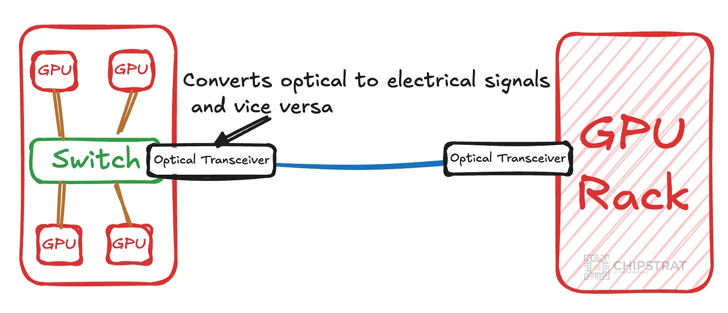
Once copper no longer works and communication moves to fiber, the system requires an electrical-to-optical conversion. That conversion happens inside the transceiver.
We covered the basics of that process here:

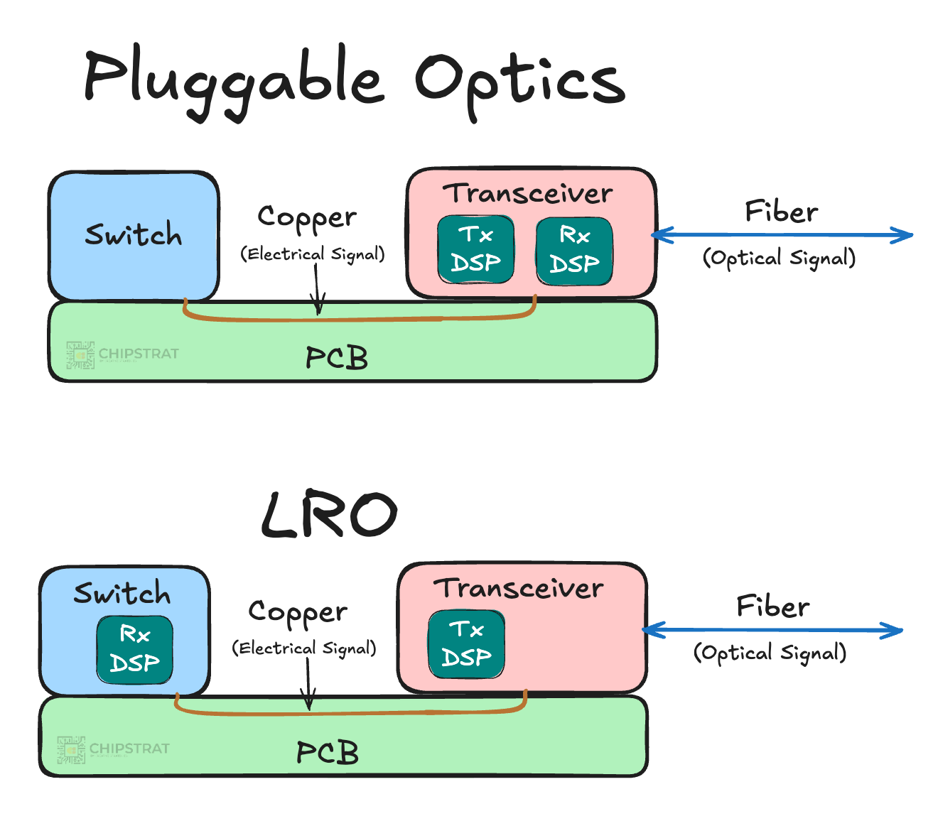
As a reminder, here’s the very high-level mental model:
Here’s a bit more of the pluggable mental model from last time:
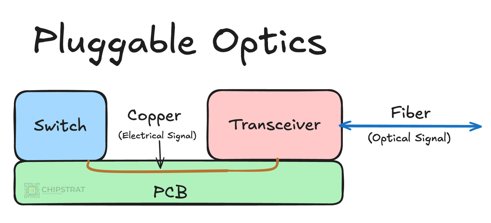
Remember that pluggable optics cleanly separate the switch from the optical link. This allows optics to be field-replaceable; if there’s a failure with the optics, you replace the transceiver module, not the switch. And if a new generation of optics arrives, you can often deploy it without redesigning the entire system. That modularity has been a major reason pluggable optics scaled so well across Ethernet generations.
However, there’s a problem with this approach. At modern rates like 50 Gb/s or 100 Gb/s per electrical lane, even that short copper path is extremely noisy.
See The Problem With Copper. This problem is conceptually similar to AECs.
To compensate for the noise introduced by the copper trace, pluggable transceivers include a digital signal processor (DSP) that equalizes and retimes the signal before and after the copper link:
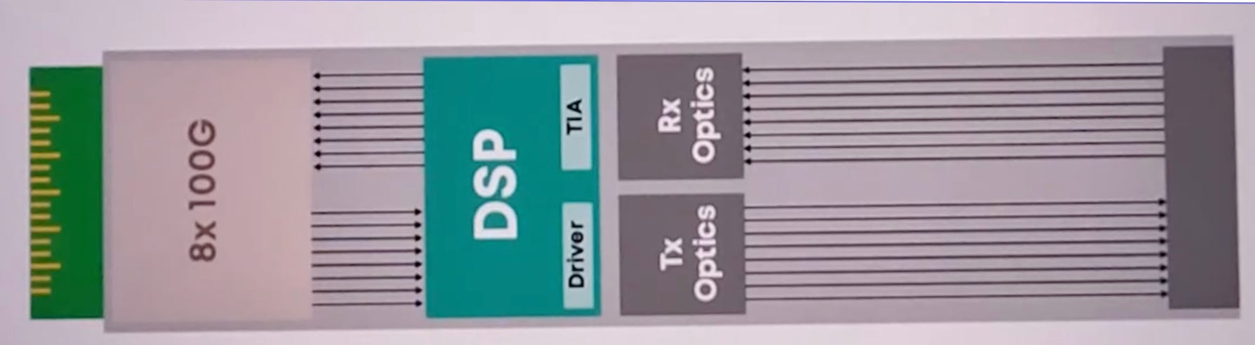
The DSP conditions the signal before it traverses the copper path between the transceiver and the switch, and does the same in the reverse direction.
But that conditioning comes at a cost. DSPs consume a meaningful amount of power. And power is the main constraint today at AI datacenter scale. If you have a cluster with thousands of transceivers, the power consumption really adds up. Every watt spent in networking is a watt not available for matrix multiplication.
DSPs also introduce additional latency through retiming and increase transceiver cost due to the added silicon. Thus, it’s interesting to ask optimization questions.
What if we got rid of the DSP? Could we put that signal processing (equalization, clock recovery, forward error correction) inside the switch ASIC instead?
That question leads to linear receive optics (LRO).
LRO (Linear Receive Optics)
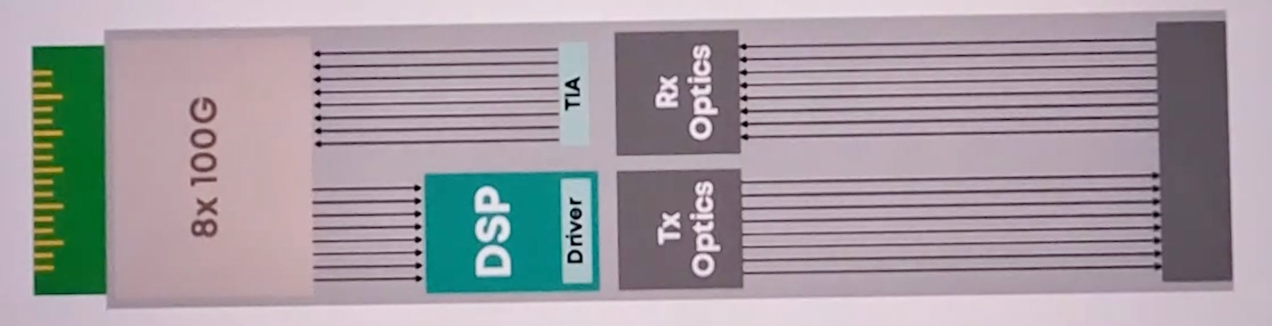
The first step to reduce transceiver power is to remove the DSP on the receive side of the transceiver:
Our mental model of the receive DSP functionality moving from the transceiver into the switch looks like this:
Now you might be wondering: why move only the receive DSP? And why call it “linear receive”? What does “linear” even mean here?
Good questions. I was wondering those myself.
In a traditional pluggable transceiver, the receive path is non-linear.
Early on, the signal is simply amplified and filtered, which is linear. But the DSP then takes over and effectively “decides” where each bit starts and whether it represents a 0 or a 1. At that point, small changes in the signal can produce completely different outputs, which is what makes the path non-linear. The “decision-making” is non-linear.
In LRO, the receive path remains entirely analog. The photodiode and transimpedance amplifier convert incoming light into an electrical signal and amplify it, but they do not recover clocks or retime data. The raw waveform is passed directly to the switch SerDes. It stays linear.
(Recall that the photodiode converts incoming photons into a proportional electrical current, and the TIA converts that current into a voltage and amplifies it. Both operations are linear in the sense that the output is proportional to the input.)
So why offload the receive only? Receive-side DSP is where most of the power and complexity live at high speeds, which is why LRO starts there. Most bang for your buck. On the transmit side, the signal originates inside the switch SerDes and is already well controlled. The switch knows its own timing, voltage swing, and encoding, so transmit conditioning is comparatively straightforward and thus requires less processing and less power.
But receiving is harder. The incoming signal has traversed a lossy channel. Recovering the clock and correcting errors requires a more sophisticated DSP that must continuously adapt to changing conditions. As lane rates climb, that adaptive receive logic dominates both power and design complexity.
So by offloading receive DSP to the switch, LRO targets the highest-impact portion of the problem first and captures most of the power savings.
There’s a tradeoff, of course.
When the receive DSP is removed, that system adaptability reduces. The switch ASIC must now handle incoming variation that was previously absorbed inside the transceiver, including multi-vendor differences across optics, boards, and operating conditions. The system becomes more tightly coupled and less forgiving, as the ASIC may not choose to support such variation.
That flexibility tradeoff can still make sense though, because LRO can deliver on the order of 30 percent power savings at the transceiver level.
Which raises the next question: if some DSP can move into the switch, why not move all of it? Wouldn’t that save the most power?
LPO (Linear Pluggable Optics)
Why not indeed. That is exactly what linear pluggable optics do:
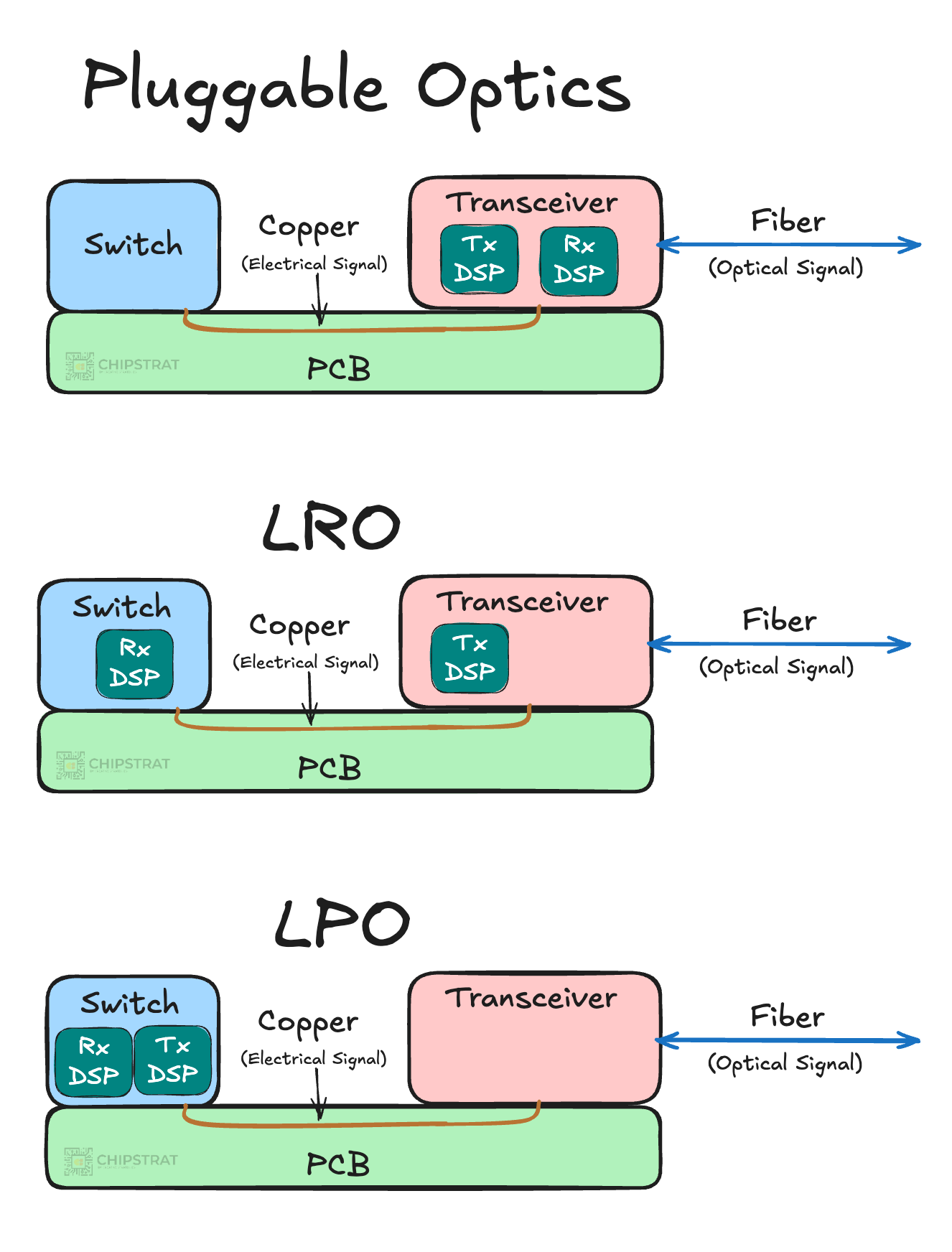
In LPO, both the transmit and receive paths are kept linear. The DSP inside the transceiver is removed or reduced to the bare minimum. The pluggable form factor is retained (good for maintainability), but all the signal conditioning responsibility is shifted to the switch.
As you would expect, eliminating the DSP reduces power and latency across the transceiver fleet. At scale, that adds up!
The tradeoff is tighter coupling. Successful LPO deployments require careful co-design between the switch, the board, and the optics. The system becomes less tolerant of variation, and the ecosystem narrows. Qualification is harder, and multi-vendor flexibility is reduced.
LPO explicitly trades modularity for efficiency. It keeps the operational advantages of pluggables while assuming a more vertically integrated system design. Hyperscalers with strong internal hardware teams are best positioned to make that trade.
Of course, you might be wondering all along: why not just deal with the real problem… that long noisy copper wire!
Yep! The real problem is the long, noisy copper trace between the switch and the optics. Moving around the DSP is a nice band-aid optimization, but why not just tackle the root of the problem?
That leads directly to NPO and CPO. As we teased in Part 1, NPO and CPO are solutions to the length of the noisy channel:
The picture pretty much says it all, but I’ll explain more the next time we revisit this series.