We’ll revisit these limits and then discuss the solution: chiplets!
SoC Problems
System-on-chips (SoCs) have become dominant by integrating multiple functions into a single die, including CPU, GPU, memory, I/O, and analog components. Apple’s M3 is a prime example, packing nearly everything onto one piece of silicon:
Apple’s M3 is an example of an SoC with logic, memory, I/O, and more all on a single chip. Source
But this approach has reached its limits. For example, yield drops as dies get larger:
This is a contrived example, but it demonstrates how both wafers have the same number of defects (marked in red) while the wafer with smaller dies results in significantly more usable chips.
Physical limits also play a role. The reticle limit—the largest area a lithography tool can pattern in one pass—caps die size at around 800 mm², and many modern SoCs aim to push past that ceiling.
Additionally, the cost of manufacturing large dies at advanced nodes like 3nm is prohibitively high, making it viable only for high-volume products. Moreover, SoCs require all components to use the same leading-edge node, even if several blocks (like analog or RF) don’t need it. Why pay for 3nm transistors when a 28nm node suffices?
How can the industry continue to move forward?
The answer: Chiplets!
Chiplets
A chiplet is a small, specialized piece of silicon designed to operate as part of a larger system.
Unlike a traditional monolithic SoC, which integrates compute, I/O, memory controllers, and analog functions into one large die, chiplets divide these functions into separate dies.
“Chiplets offer a modular system that combines separate chips from different vendors and technology nodes instead of designing all functions into one monolithic system on chip.” Source
A chiplet-based design integrates multiple specialized dies into a single package, forming a unified system. Each chiplet can utilize the process node that best suits its function, such as 3nm for logic or 28nm for analog, thereby maximizing cost-effectiveness, performance, and power efficiency.
What are systems of chiplets called? You’ll often hear the term multi-chip module (MCM), which is a package that contains multiple separate dies (chiplets) interconnected on a single substrate.
Advanced packaging techniques like 2.5D interposers and 3D stacking with hybrid bonding connect chiplets, enabling high-bandwidth, low-latency links between chiplets.
AMD EPYC example
AMD was the first to bring chiplets into mainstream production, offering a deep and well-documented case study on how modular design can scale in the real world. So let’s start there!
AMD EPYC servers feature a modular MCM design. AMD’s CPU and I/O dies are combined to create SKUs tailored for varying needs, from value offerings with only eight cores to high-performance models with 192 cores:
AMD explains why it pursued a chiplet approach and how it uses different process nodes for different die:
The most industry-influential innovation in AMD EPYC processors is the hybrid multi-die architecture first introduced with second generation EPYC processors. We anticipated the fact that increasing core density in monolithic processor designs would become more difficult over time. One of the primary issues is the fact that the process technology for CPU cores are on different innovation paths than the technology that lays down the analog circuitry to drive external pathways to memory, I/O devices, and an optional second processor. These two technologies are linked together when creating monolithic processors and can impede the swift delivery of products to market.
Nice! Using different process nodes appropriately. AMD continues,
AMD EPYC processors have decoupled the innovation paths for CPU cores and I/O functions into different dies that can be developed on their own timelines and produced with process technologies appropriate for the tasks they need to accomplish. Generation over generation, we have pushed the size of CPU dies smaller as process technology allows (Figure 1). Today’s ‘Zen 5’ cores are produced using 4nm process technology, the ‘Zen 5c’ core is produced at 3nm, and the I/O die remains at 6nm from the prior generation. This allows them to address diverse workloads, from minimal-core systems to compute-dense servers.
Believe it or not, the idea isn’t new. In Gordon Moore’s seminal 1965 article, he speculated that “it may prove to be more economical to build large systems out of smaller functions, which are separately packaged and interconnected”.
Moore was right!
What Chiplets Enable
As the AMD EPYC example demonstrates, a chiplet-based system offers many advantages.
Higher Yield, Lower Cost
Chiplets are small, and smaller dies improve wafer yields since the chance of a defect affecting a die diminishes with size. In a monolithic SoC, a single flaw can render the entire chip unusable. However, with chiplets, more functional dies can be obtained from each wafer, reducing the effective cost per chiplet. Improvingyield is a great way to reduce per-unit costs.
Reticle-Limit Bypass
The photolithography reticle sets a hard size limit on a single die. But chiplets allow designers to sidestep that barrier. Systems like AMD’s MI300A and MI300X achieve significant FLOPS by combining multiple chiplets into one package, essentially stitching together a system larger than a single reticle can handle.
Note the visual similarities between the MI300A and MI300X! This image visually articulates the value proposition of chiplets, demonstrating the reuse of existing IP.
While not chiplets in the strict sense, Nvidia also bypasses the reticle limit, tying two “reticle-sized” GPU die into a single unified GPU:
This is a modular multi-die design with two reticle-limited dies linked by a 10 TB/s interconnect. It’s not chiplets in the strict sense, but spiritually it’s the same idea: partitioning the system into chips and reconnecting the pieces with high-bandwidth packaging.
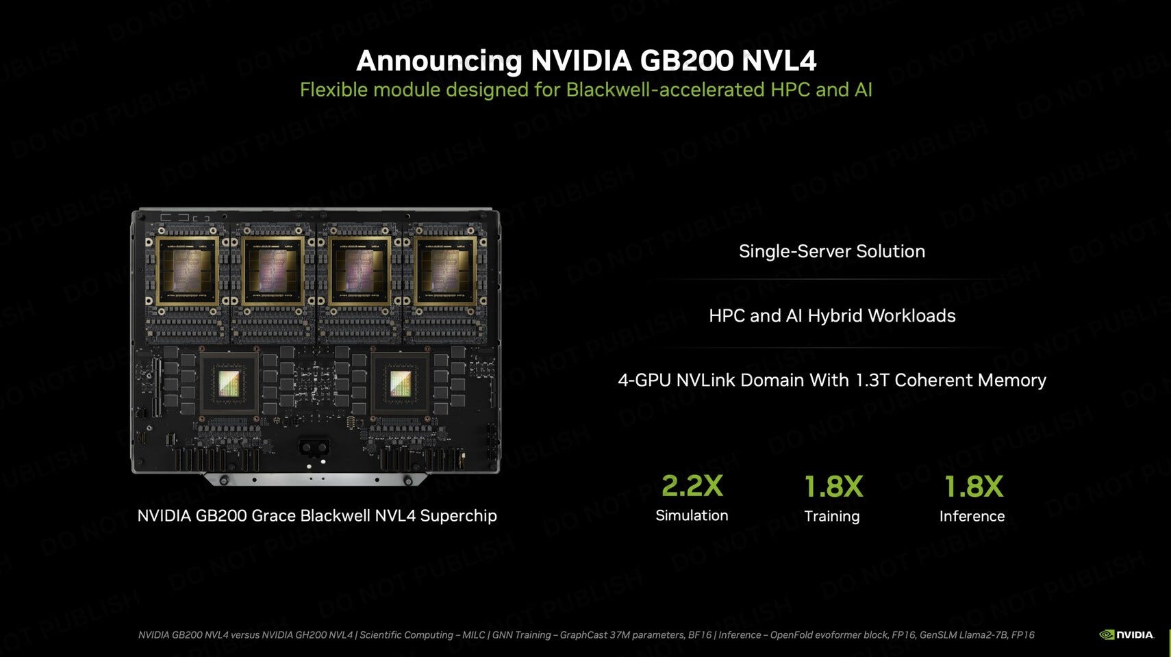
Nvidia can then compose systems like GB200 NVL4 with four reticle-sized GPUs and two smaller Grace CPUs powered by Arm’s Neoverse V2 cores:
Process Node Optimization
As we saw with the AMD EPYC example, chiplets enable heterogeneous integration, a form of “mix-and-match” process technology that was previously impossible in monolithic SoC designs. Each chiplet can be built on the most suitable node; no need to force everything onto the latest process.
Design Reuse
Once a chiplet is validated, it becomes a reusable design block, conceptually similar to an IP block in an RTL library. A proven I/O chiplet, for example, can be integrated into multiple product lines with significantly reduced design effort compared to developing new silicon from scratch, amortizing the original NRE (non-recurring engineering) cost across many SKUs. Yes, system-level verification and integration work are still required for each new product. Yet this approach saves substantial time and money while reducing design risk.
Note that the degree of chiplet reusability depends heavily on interface standardization and system compatibility. Chiplets with well-defined, standardized interfaces (such as those following UCIe specs, which we will discuss below) offer the most significant reuse potential. In contrast, those with custom interfaces may require additional adaptation work for each integration. System-level considerations, such as power delivery, thermal management, and signal timing, must still be validated for each new product configuration; however, core functionality verification is already complete.
Design reuse is what makes everyone excited about chiplets and was a key component of AMD’s turnaround strategy, enabling it to punch above its weight. AMD CTO Mark Papermaster explained
Mark Papermaster: We began restoring our CPU roadmap about a decade ago. We reengineered our engineering processes, and one of the things we settled on was a more modular design approach, where we develop reusable pieces that we could then put together based on [an application’s] needs.
While early adoption has come from leaders like AMD and Intel, the design reuse benefits of chiplets could lower the barrier for smaller fabless teams to build custom silicon.
Faster Time-to-Market
Leveraging design reuse enables companies like AMD to go to market faster. Proven chiplets (like AMD’s CPU core) can be dropped in without redesigning the entire SoC.
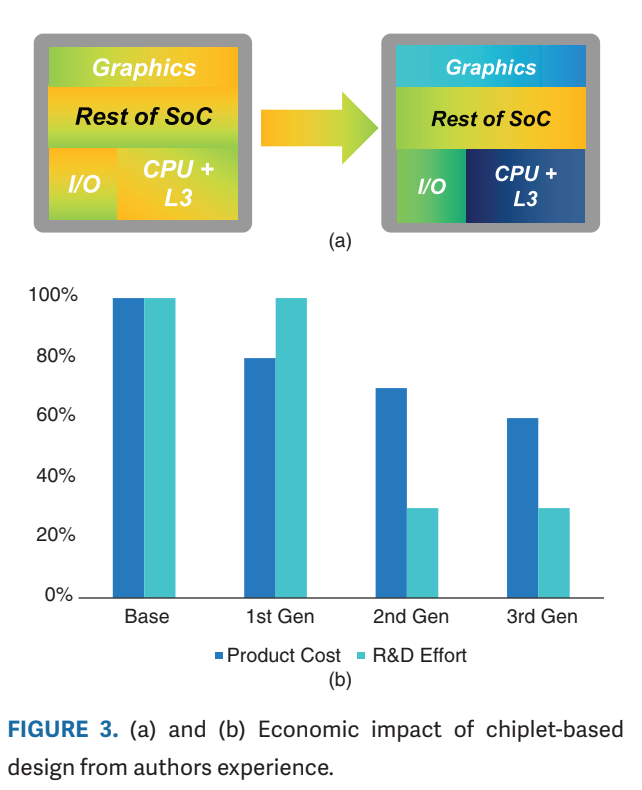
As Cadence points out, building the first chiplet-based product takes work, but future iterations benefit from much shorter time-to-market:
Source
In the first go-around, there is the overhead of designing for a disaggregated architecture, but subsequent generations benefit significantly with reduced development cost and increased choice of SKU generation, as shown in Figure 3(b).
Again, reuse also lets companies amortize development costs across multiple products. Once a high-performance chiplet is built, it can slot into many designs, accelerating development and reducing NRE.
This modular approach offers strategic flexibility. By assembling systems from pre-validated chiplets during the design cycle, known as late binding, companies can delay final SKU decisions until production. This enables responses to shifting customer needs or last-minute hardware changes without full redesigns.
What if companies could even sell those chiplets to others?
More Examples
The theoretical benefits of chiplet-based systems include improved yield, reduced costs, optimized processes, quicker iterations, and scalable reuse, leading to a more flexible and efficient model for chip design.
Here are more examples that showcase these benefits.
Startups, too!
Currently, the benefits of chiplets are primarily enjoyed by the largest companies. But smaller companies want in on the future too!
See this example from Ampere. Well, Ampere *was* a startup until it was acquired by SoftBank two months ago.
Ampere’s AmpereOne platform uses chiplets to disaggregate compute, memory, and I/O, optimizing each for power, performance, and process node:
The compute die, built on TSMC’s 5nm, contains 192 custom Arm cores. Memory and PCIe controllers are split into separate 7nm I/O dies.
This modular design lets Ampere build multiple SKUs using the same core silicon. For example, the only difference between AmpereOne and AmpereOne M is the addition of two memory dies. No new compute die is needed. This approach enables customers to scale performance and I/O without a complete redesign, thereby reducing time and cost.
This is precisely the benefit of chiplets!
In another example, startup d-Matrix has built its Corsair inference platform entirely around a chiplet-based architecture, using 16 small dies per dual-card system.
d-Matrix scales memory and compute by using smaller chiplet dies that improve yields, lower costs, as well as overcome reticle limits.
Equally important, d-Matrix can flexibly mix and match chiplets to keep pace with evolving AI workloads, without requiring the redesign of monolithic chips. Their architecture supports both low-latency inference for small interactive models and high-throughput compute for large batch jobs, all on the same modular silicon foundation.
AMD MI300A example
Diving deeper into MI300A serves as another tangible example of the advantages of chiplets.
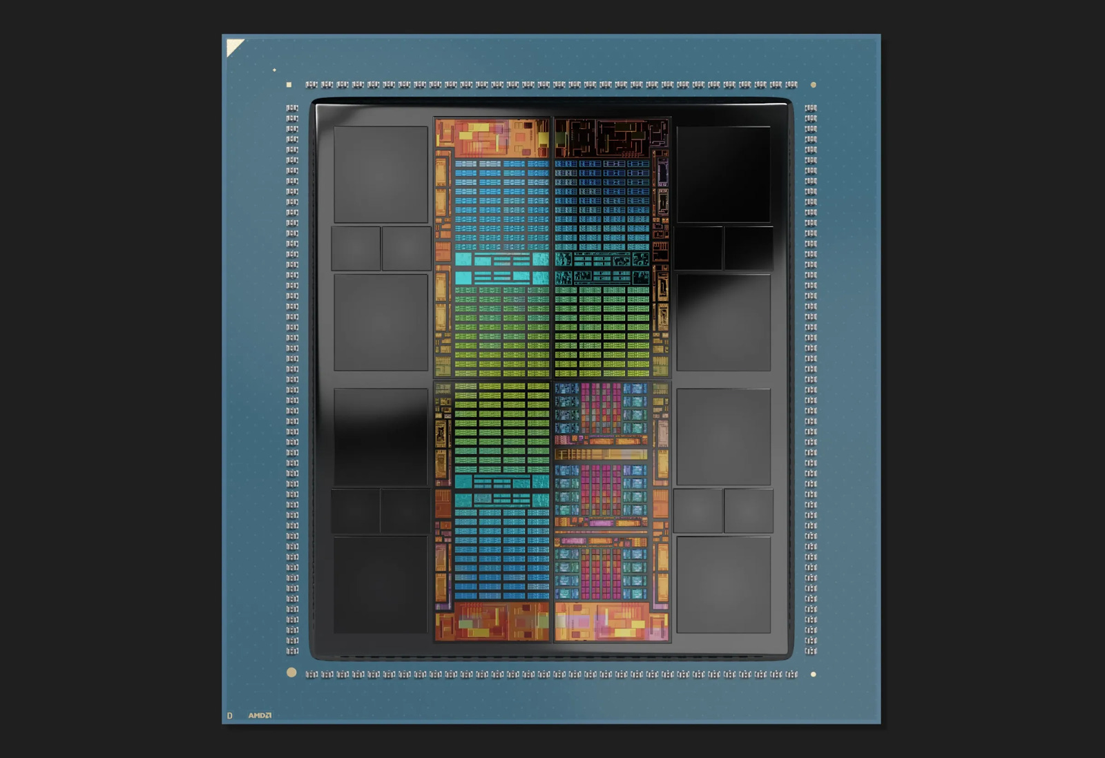
AMD MI300A. The black squares around the edge are HBM. In the middle two colorful columns, the left column has four XCDs (accelerator dies), and there are two more on the top of the right column. The bottom right colorful column has three CCD (CPU dies). The other colorful bits are I/O die.
MI300A bundles the CPU chiplet (CCDs) with AI accelerator chiplets (XCDs). These die are made with the leading edge fabrication process, yet the system also packages together I/O dies (IODs) made from a previous process node.
The MI300A reuses CPU chiplets (“Zen 4”) that were also used in EPYC CPU servers!
“Breaking the GPU into chiplets allowed us to put the compute in the most advanced process node while keeping the rest of the chip in technology that’s more appropriate for cache and I/O,” he says. In the case of the MI300, all the compute was built using TSMC’s N5 process, the most advanced available and the one used for Nvidia’s top-line GPUs. Neither the I/O functions nor the system’s cache memory benefit from N5, so AMD chose a less-expensive technology (N6) for those. Therefore, those two functions could then be built together on the same chiplet.
Here’s a rotated, annotated image of those colorful center columns, which have XCDs (accelerator chiplets), CCDs (CPU chiplets), and IOD (I/O die).
And proprietary chiplets aren’t the only avenue in town.
It’s possible to license IP when making chiplets too. Here are some examples across the spectrum of fabless designers using Arm in chiplet-based designs.
Amazon’s Graviton 3 & 4
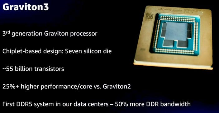
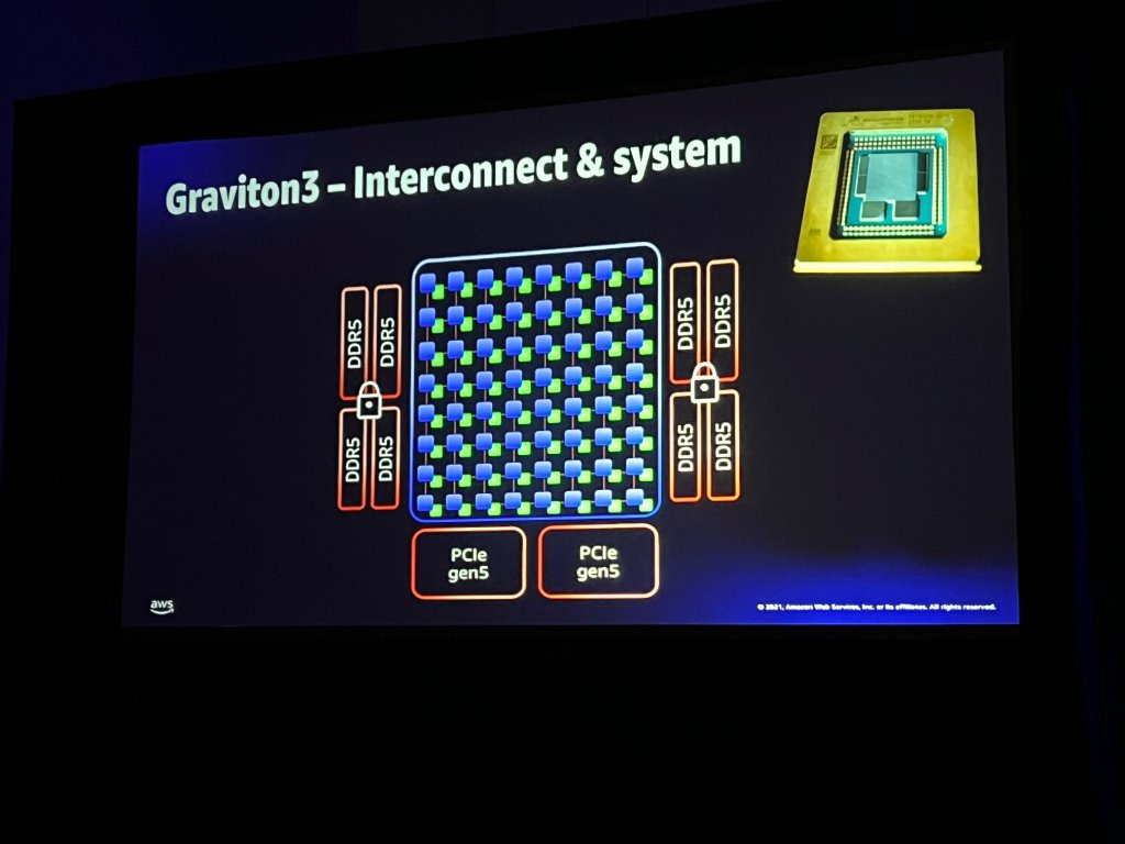
Amazon’s Graviton3 processor is a case study in chiplet use at a hyperscaler. And Amazon’s compute chiplets aren’t proprietary, but leverage IP from Arm:
According to SemiAnalysis, at its core is a 64-core compute die built on a leading-edge node using Arm’s Neoverse V1 cores. Surrounding it are six I/O chiplets: four DDR5 memory controllers and two PCIe 5.0 controllers, each fabricated on mature, cost-effective process nodes.
A big compute chiplet surrounded by I/O chiplets. Source
By moving the I/O onto separate chiplets, Amazon avoids cramming everything onto one piece of silicon. This helps the processor stay cooler and use less power, about 100 watts, which is far lower than most competing CPUs.
Note that Amazon didn’t try to reinvent the wheel when it came to the processor core. Instead of designing one from scratch, per SemiAnalysis it used a proven design from Arm called Neoverse V1.
The Neoverse V1 CPU is designed to deliver leading per-core performance on demanding HPC, HPC in the cloud and AI/ML-assisted workloads
Leveraging Arm IP allowed Amazon to focus on areas where it could make a significant difference—how the system is partitioned into chiplets, how those components are packaged, and how the entire system is designed, built, and deployed.
According to The Next Platform, AWS’ next-generation Graviton 4 continues the chiplet approach:
Graviton Gen1 through Gen4.
In a future post, we’ll explore how Arm is formalizing this modular approach with its Chiplet System Architecture—and what that might mean for the rest of the industry.
But, like everything, disaggregated design with chiplets has its own set of trade-offs.
New Problems Chiplets Introduce
Chiplets solve many of the problems inherent in monolithic SoCs, but they create new ones too. Breaking a system into multiple dies introduces fresh challenges in power delivery, communication, and packaging. Every die boundary becomes a new interface to engineer, validate, and maintain.
Communication Overhead
Interconnects between chiplets add latency and power overhead. Off-die links are slower and less power-efficient than on-die wires. Signals that once traveled short metal layers must now cross package substrates or interposers, adding latency and energy overhead.
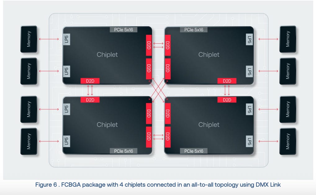
Here’s a nice illustration of different ways to connect chiplets:
This off-die communication can be significantly more power-hungry than on-die interconnects. We’ll dive deep into advanced packaging, i.e. connecting chiplets, in a future post.
Power Delivery
Power delivery becomes harder in chiplet-based systems too. Each die may have different voltage levels, current draws, and transient behaviors, especially when built on different process nodes or designed for different roles like compute, memory, or I/O.
In a monolithic SoC, power moves through a unified metal stack, offering compact, low-impedance delivery. But in a disaggregated system, power must cross bumps, microbumps, and/or interposers. These longer paths introduce IR drop and reduce voltage precision. As a result, power delivery becomes noisier and less efficient, requiring careful package co-design.
Thermal Management
Thermals also get more complicated.
These chiplets often run different workloads, use different process nodes, and generate uneven amounts of heat. This creates scattered thermal hotspots rather than a smooth thermal gradient, making it harder to cool the system effectively.
Managing heat becomes a more complicated problem, especially with 3D stacking.
Packaging Complexity
Chiplets only work if packaging connects them into a coherent system. That means advanced technologies: 2.5D interposers, silicon bridges, 3D stacking, and hybrid bonding. This can add cost, yield, and reliability burdens to the package.
System performance increasingly depends on advanced packaging. Packaging has never been more important!
Tooling, Standards, and Ecosystem
This emphasis on packaging impacts the semiconductor value chain. Foundries, OSATs, and EDA vendors are no longer support actors, but they’re becoming strategic partners. Designing, validating, and assembling chiplet systems demands new tooling, tighter collaboration, and end-to-end integration flows. Want to design a chiplet-based system? Sure, but your EDA tool needs to support that!
Test infrastructure must adapt too! Known-good-die testing becomes essential, as any failed die can compromise the entire system. Thorough validation before integration is critical for cost control.
Even security models must evolve! With chiplets, each die is a potential attack surface. What if a third-party die was built using a compromised supply chain? Could it have a backdoor? We’re early in the chiplet marketplace concept, but watch for themes like security as the use of third-party die increases.
Standardizing physical and electrical interfaces isn’t enough. To make chiplets truly modular, they also need common software and firmware layers. Chiplets must expose their capabilities, be discoverable by the system, and interoperate reliably. As the ecosystem matures, reusable firmware and pre-integrated software stacks will be as critical as the hardware itself.
Complexity
Ultimately, chiplets add system-level complexity, now at the package level.
Interconnect Standards Matter
Early on, large designers like AMD jumped in and brought chiplets to reality. This involved building custom interconnects (like AMD’s Infinity Fabric). However, the long-term goal of the semiconductor industry is to create an ecosystem where any fabless designer can reap the benefits of chiplets.
Standards make chiplets interoperable. They enable companies to purchase from various vendors and speed up development. In the absence of standards, chiplets remain confined in silos, but with standards in place, chiplets transform into genuine “Lego blocks”—reusable, interchangeable, and scalable.
UCIe
Universal Chiplet Interconnect Express (UCIe) is one such open standard designed to bring chiplets the kind of interoperability PCIe brought to expansion cards. It’s packaging-agnostic, supporting everything from low-cost organic substrates to 2.5D interposers and silicon bridges. That makes it viable for both budget-friendly and high-performance designs.
UCIe covers the full die-to-die stack: the physical layer (how signals move between dies), the protocol (how data is transferred), and the software model (how chiplets are discovered, managed, and programmed).
Plug-and-Play Ecosystem
By standardizing how chiplets connect, UCIe opens the door to a true chiplet marketplace. Without shared interfaces, chiplets stay locked inside each vendor’s ecosystem. However, with a common standard, companies can specialize in building the best compute, memory, or I/O dies, knowing their parts will work in broader systems. For system designers, that means more flexibility, faster development, and more choice.
This shift also reshapes the supply chain. Instead of building everything in-house, companies can source chiplets from specialists in each domain. It’s a modular approach that accelerates development and fosters third-party innovation.
The long-term vision is a chiplet marketplace: verified, interoperable dies available off-the-shelf and ready to be assembled like Lego. Think of it as IP blocks in silicon form.
But standards alone will not deliver that vision. A marketplace also requires a trusted third party to define a shared architecture, enforce compliance, and coordinate contributions across the entire stack from hardware to software.
Arm’s Chiplet System Architecture outlines a standardized approach to breaking down chips and connecting their components. It covers not only how chiplets communicate with each other, but also how they integrate across hardware, software, and system design. While UCIe handles the physical link between chiplets, Arm’s approach focuses on how they work together as one system. We’ll explore this further in a future post—it could help turn chiplets into truly mix-and-match building blocks.
Closing
Chiplets represent the next chapter in chip design and manufacturing—what I refer to as the “disaggregated design” era.
Rather than cramming everything onto a single chip, designers can now split systems into smaller modules, each built for a specific task and often manufactured on the most efficient process available.
As standards gain traction and trusted players like Arm step in to guide integration, we may see a true chiplet marketplace emerge—where parts from many vendors come together as easily as building blocks.
In the coming years, we’ll see a shift in how chips are built, delivered, and sold.
Chipstrat is a reader-supported publication. To receive new posts and support my work, consider becoming a free or paid subscriber.
Also, if you liked this post, check out Vik’s recent and related article on advanced packaging: