

The Long Arc of Semiconductor Scaling
The journey from vacuum tubes to transistors, from small ICs to billion-transistor SoCs. Setting the stage for chiplets.

I planned to write a chiplets explainer this week while traveling to and from CadenceLIVE in San Jose… but I got sucked into the broader chiplets backstory while doing research. After all, chiplets are a semiconductor manufacturing and scaling story of sorts!
So I’m pivoting. This post shares the fun historical arc of transistor and IC scaling and concludes with the problems chiplets set out to overcome. A future post will pick up where this leaves off, discussing chiplets and their trade-offs.
So sit down, relax, and enjoy the show!
Goodbye Vacuum Tubes, Hello Solid-State Electronics
The story of semiconductor scaling begins with the earliest discrete transistors, connected to make simple circuits like this:
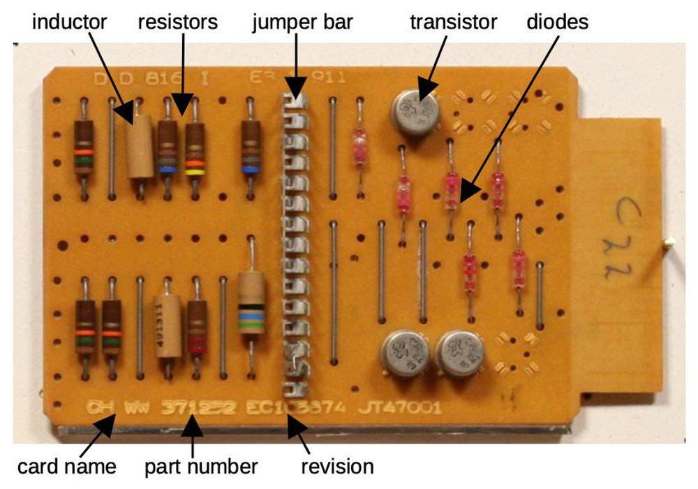
Notice how this system has three transistors, each residing in its own package.
Although quaint by today’s standards, this transistor-based logic was a welcome replacement for big, unwieldy, unreliable vacuum tubes. Check out this vacuum tube logic circuitry found in an IBM 704, a 1950’s digital computer. Note the vacuum tubes on top:

It’s honestly a bit shocking to me to imagine this vacuum-based computing even worked! As the University of Waterloo museum recounts,
This is a vacuum tube module for the IBM 704 system. You can see of a row of 6 vacuum tubes with a mechanical relay in between them. In later iterations the relay was replaced by two more vacuum tubes for a total of eight. The tubes were part of the logic circuitry. IBM sold the 704 computer from 1954 to 1960. It was a 'scientific' computer, intended for complex calculations, and one of the earliest to use core memory. The FORTRAN and LISP programming languages were originally developed for the IBM 704.
LISP and FORTRAN could run on this prehistoric thing? That is WILD!
The Invention of the Transistor
These big vacuum tube systems were unwieldy and unreliable, yet AT&T Bell Labs successfully used them in its telephone systems. That said, Ma Bell really wanted to get rid of these cumbersome tubes. From Jon Gertner’s fantastic book The Idea Factory: Bell Labs and The Great Age of American Innovation,
In a [telephone] system that required supreme durability and quality, there were, in other words, two crucial elements that had neither: switching relays and vacuum tubes.
They were delicate mechanical devices; they used relays that employed numerous metal contacts; they could easily stop working and would eventually wear out. They were also, because they clicked open and closed, far slower than an electronic switch, without moving parts, might be.
Kelly had set an intriguing goal that lingered in [William] Shockley’s mind as he finished his indoctrination program and turned back to studying the physical properties of solid materials on his own and with his study group. Kelly’s articulation of a solution—a product, in essence—was fairly straightforward, even if the methods for creating such a product remained obscure: Perhaps the Labs could fashion solid-state switches, or solid-state amplifiers, with no breakable parts that operated only by way of electric pulses, to replace the system’s proliferating relays and tubes. For the rest of his life Shockley considered Kelly’s lecture as the moment when a particular idea freed his ambition, and in many respects all modern technology, from its moorings.
Shockley started researching semiconductor materials as a possible solution, way back in 1939 before World War II:
Shockley had concluded by then that a certain class of materials known as semiconductors—so named because they are neither good conductors of electricity (like copper) nor good insulators of electricity (like glass), but somewhere in between—might be an ideal solid replacement for tubes. Under certain circumstances semiconductors are also known to be good “rectifiers”; that is, they allow an electric current passing through them to move in only one direction. This property made them potentially useful in certain kinds of electronic circuits. Shockley believed there could be a way to get them to amplify a current as well. He intuited that one common semiconductor—copper oxide—was a good place to start.
After the war, Shockley returned to semiconductor amplifier research, but this time, he and his team decided to explore silicon and germanium instead of copper oxide.
Indeed, this was the situation Shockley confronted upon his return to Bell Labs, as he began working with his solid-state physics group. His team could have continued working with a semiconductor such as copper oxide, which was what Shockley and Brattain had tinkered with before the war. But early on, the solid-state group decided they were interested in understanding better what seemed to them the most fundamental and representative materials in the class. “Although silicon and germanium were the simplest semi-conductors, and most of their properties could be well understood in terms of existing theory, there were still a number of matters not completely investigated,” an internal history of the solid-state research project later explained.
Yet expectations for these materials were low.
Germanium had been discovered in Europe in the late 1800s, and as with silicon, wafers made from the element had proven useful during the war for radar detectors. The small amounts the men worked with came from tiny military stockpiles in Missouri, Oklahoma, and Kansas. Silvery and lustrous in appearance, germanium was so rare that one Bell Labs scientist remarked that before 1940 only a handful of people in the world had actually ever seen it.
Looking back, it wasn’t obvious that germanium would pan out, but it proved to be a good choice. John Bardeen and Walter Brattain achieved the first successful semiconductor amplifier in December of 1947.
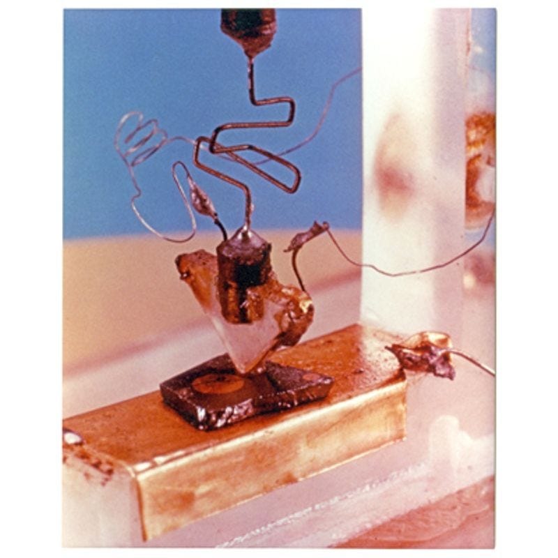
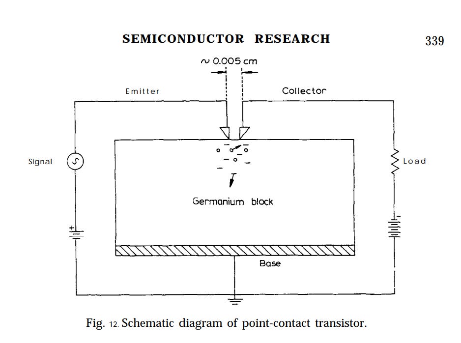
It’s not quickly apparent what’s going on in that picture, so here’s a schematic from John Bardeen’s 1956 Nobel lecture. (Visit that link for an in-depth explanation too.)
This crude device could do the impossible: amplify voice without vacuum tubes!
On Christmas Eve 1947, Brattain wrote an account of the previous day’s events in his notebook. Amid the lined pages, he made a quick drawing of the amplifier he had built. He drew another diagram of the device after he and some colleagues had arranged for a voice signal to pass through the circuit that ran through this ugly little amplifier. Brattain wrote, “This circuit was actually spoken over and by switching the device in and out a distinct gain in speech level could be heard.” There was no noticeable change in quality. The power gain was eighteen times or more.
Semiconductor transistors had arrived!
In [Bell Lab’s VP of research] Bown’s personal account of the episode, he admitted that he was immediately convinced the device was not only real but important. It was, he privately suspected, more than an amplifier, more than a switch, more than a replacement for the vacuum tube. But on Christmas Eve, with the year almost over and with a powerful snowstorm bearing down on the East Coast, knowing precisely what it portended, or indeed how it all fit together, would require some serious consideration, as well as some time. Bardeen and Brattain’s device, Bown simply noted, was “a basically new thing in the world.”
Basically a new thing in the world.
Amazing.
Out of the Lab, Into Production
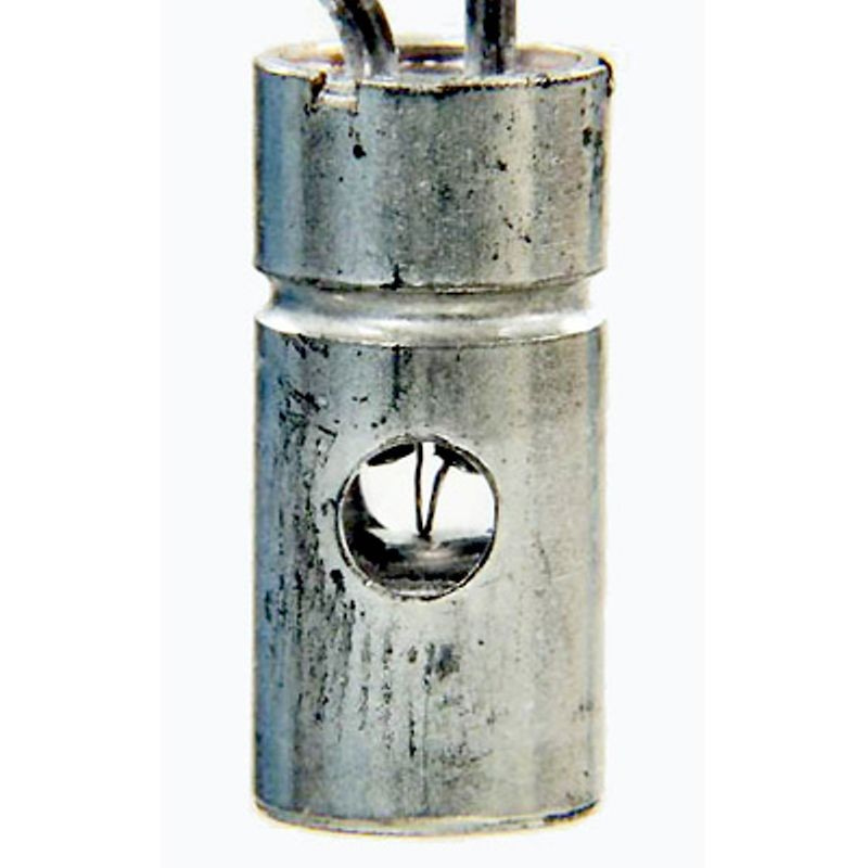
Bell Labs improved upon their initial transistor design by housing the prototype in a more durable, though still delicate, metal cartridge, creating what became known as the 'Type A' transistor. Production ran into the thousands.
However, these transistors were bulky and brittle, so transistor architecture and manufacturing research continued. Could they be made smaller and more reliable?
Between AT&T Bell Labs deciding to license the transistor technology, Shockley’s 500-page masterpiece, transistor technology quickly diffused. Many companies got in the game and helped advance semiconductor research and manufacturing:
By the time Jack Morton had ironed out some of the production problems with the point-contact transistor in the early 1950s, the Labs was ready to move ahead in licensing the technology. Shockley, seemingly immune to normal human fatigue and now without question the most eminent solid-state physicist in the world, had already written and published a five-hundred-page book—Electrons and Holes in Semiconductors—that would serve for decades as a definitive guide to scientists and engineers working with the new materials. And in 1951 and 1952, the Labs began sponsoring multiday conventions at Murray Hill, attended by hundreds of scientists and engineers from around the world, who were interested in licensing transistor rights. At the conventions, Jack Morton gave the guests a brief overview of the transistor and Gerald Pearson followed with a brief tutorial on transistor theory. The next two days were given to in-depth presentations on different types of transistors and their applications. The cost for licensing the transistor technology was $25,000. A free exception was made for companies that wanted to use the devices for hearing aids. This was in deference to AT&T founder Alexander Graham Bell, who had spent much of his career working with the deaf.
Not only could one license the technology, but they could attend a workshop to learn all about it from the inventors!
By the way, the Shockley book mentioned above was responsible for TSMC founder Morris Chang’s semiconductor education! From Acquired,
David: Anyway, back to this moment in time. Morris is just studying the Shockley textbook in his hotel room, but he’s not in college and he doesn’t have any teachers. He just has the book, but he’s very resourceful. He figures out that one of the senior engineers at the plant is an alcoholic and hits up the hotel bar almost every night.
What Morris does is he comes home from work in the early evening, he studies in his room for a couple of hours, and then later at night when the older colleague shows up at the bar, Morris goes down to the bar not to drink, but he brings the textbook and he asks the guy questions. He’s like, I don’t understand this, I don’t understand that. He’s just like buying drinks for his buddy. So great.
Ben: Incredible.
David: Here’s the quote he says later (he, being the older colleague), “Didn’t solve all my problems, but he solved enough so that I could move ahead. He was my main teacher about electrical engineering.” So great.
Solid-State Electronics
The advent of the semiconductor transistor ushered in the era of solid-state electronics. Transistors replaced bulky vacuum tubes, resulting in smaller, more energy-efficient, and ultimately cost-effective electronics; the radio transformed from an appliance to a handheld device.
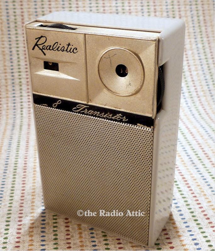
Sony was a Bell Labs transistor licensee and helped fuel the ascent of the transistor radio, the first portable consumer electronics product. The Sony episode of Acquired gives a glimpse of how the Bell Labs transistor diffused into the broader world:
David: in 1952, Ibuka [Sony co-founder Masaru Ibuka] heard that the world-famous, renowned institution that everybody respects, especially nobody more than Ibuka and Morita [Sony co-founder Akio Morita] in Japan—Bell Labs—that the then-parent company of Bell Labs, which is a company called Western Electric. It went through a whole bunch of owners, it was all related to AT&T and the various entities as part of that. That they were going to open up the transistor for international licensing. Of course, they had created the transistor in Bell Labs that they were going to license the technology internationally.
David: Keep in mind what we were saying for the last few minutes here about the size of these various technology "products" that were being used to build the radios that were the size of console tables and tape recorders the size of nightstands.
The transistor is available for license and Ibuka is like — this is it! Just like when he saw the tape recorder and just like when he got obsessed with radios before, he's like, we got to do this. Morita is like, okay. Morita goes off to New York—this is, I believe, in 1953—and negotiates a deal. It ends up taking about a year to finalize this, but he negotiates a license from Western Electric, Bell Labs, to use the transistor.
The Bell Labs guys are like, well, what are you going to do with it? Ibuka and Morita are like, we're going to make miniature radios with the transistor. They're like, guys, you can't do that. This stuff is still done with germanium at this point. You can't get enough power in this to really power a radio that would actually work. We think the market application that makes sense here is hearing aids.
Ben: Hearing aids, that's right. Ibuka and Morita are like, no, the hearing aid market in Japan will not be a viable one for us. In fact, I think there's a cultural issue where it's perceived as a weakness to be hard of hearing.
David: They knew for lots of reasons that there was no chance that they could build a big company and a big product making hearing aids.
Ben: They're betting the farm here on, we are going to be able to figure out how to dope these transistors, use a different material, or something in order to make it viable to create a radio.
David: They're nothing if not confident. Bell Labs is like, all right, good luck, guys. It takes two years, but two years later in August of 1955, TTEC [Tokyo Telecommunications Engineering Corp, predecessor to Sony] releases their first transistor radio product—the TR-55 portable radio.
And check out Sony’s beautiful product. No wonder Steve Jobs held Sony in such high regard!
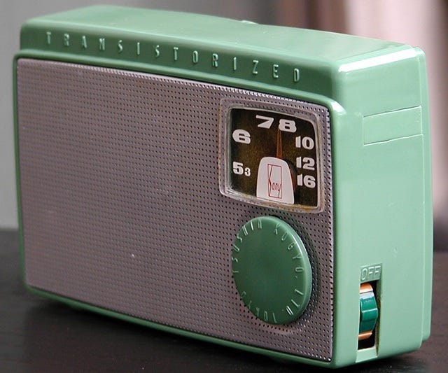
Here’s the inside. No vacuum tubes, just germanium transistors! [Source]

By the way, discrete germanium transistors are still in use and coveted for guitar pedals. This video explains (start at ~1:25):
Back to antiquity: surely electronics designers of the day had to be thinking: what could we do with more transistors? Some big projects were in the works.
Scaling Up Discrete Transistor Systems
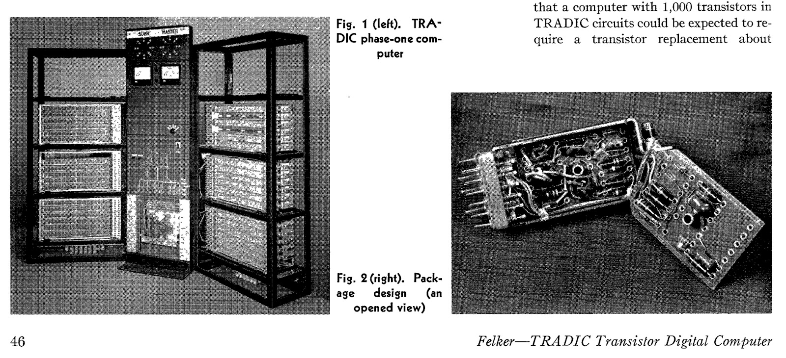
One such example: in 1954 Air Force requested Bell Labs to develop a transistor digital computer for “airborne use” (weapons?) resulting in the TRADIC (TRAnsistorized DIgital Computer), the first computer without vacuum tubes.
TRADIC used 7000 germanium transistors complemented by 11,000 germanium diodes! According to the 1954 paper Performance of TRADIC Transistor Digital Computer:
In January 1954, we completed a breadboard computer which is known as the TRADIC phase-one computer. This machine multiplies or divides in less than 300 microseconds and adds or subtracts in 16 microsecond. It is a serial machine and employs a 16-digit word length. It runs on less than 100 watts of power. The main supply voltage is 8 volts. Auxiliary bias voltages of 2 and 6 volts are also required. The machine uses a group of electric delay lines for its internal memory. It has 18 such electric delay lines each of 1-word capacity. It has provision for 13 16-digit constants which are stored in toggle switches. The program is stored in a plug board.
The TRADIC phase-one computer is a complex machine. It has 700 point-contact germanium transistors and 11,000 point-contact germanium diodes. There are 6,000 resistors and 4,000 capacitors and more than 1,000 transformers.
TRADIC is inspiring, but in hindsight it’s obviously very large and unwieldy. This isn’t going to fit into aircraft (missiles?) for the Air Force:
Interestingly, at the time, physically scaling transistor dimensions to ever smaller sizes wasn’t obvious. From the same 1954 TRADIC paper, the computer architect was banking on increased cleverness of architectural design:
Three years ago, I made certain predictions which I have reviewed before undertaking any new ones. At that time, I felt that 400 or 500 transistors might be put in a cubic foot, and this density has been achieved. Within the next three years, it should become possible to put five times that many transistors and associated circuits in a cubic foot. This advance will come about not from using smaller transistors, but by realizing equivalent performance with fewer associated components.
That’s pretty common – focusing on cleverness instead of scaling. (Kind of rhymes with Richard Sutton’s bitter lesson.)
Interestingly, though, the author suggests the need for 3D packaging. What’s new is old!
The TRADIC phase-one packages are complex circuits. There are approximately 40 parts per transistor. The package density will also be increased, of course, as we improve understanding of what we have sometimes called the microconnection problem—that is, the problem of making, say, one million connections in a cubic foot. To do this, we must surrender the convenience of two-dimensional mounting of parts and make full use of all three dimensions. We must do this, of course, in the interconnecting wiring as well as within the packages. A real obstacle is that we do not have a three-dimensional equivalent of the two-dimensional printed circuit board.
Anyway, the point here is that scaling up the number of transistors is clearly useful for computing in the early 1950s, but it wasn’t clear how to manufacture such systems with thousands of discrete germanium transistors and corresponding components.
Integrated Circuits
So far, electronics scaled down in size from large vacuum tubes to smaller discrete transistors. But can the transistors themselves get smaller?
The key insight (in retrospect) is that the transistors are large in part due to all that packaging. If every transistor is made of the same material, why make separately packaged transistors? Could they be packaged together? What if they shared a substrate?
What if the transistor is *in* the substrate instead of on the substrate?
I’m making it simple straightforward, yet it was anything but. For example, how the industry switch from germanium to silicon?
In the 1950s, a flurry of innovations from from companies including Bell Labs, Fairchild Semiconductor, and Texas Instruments made possible the manufacturing techniques and transistor architectures that ultimately made silicon-based integrated circuits viable.
First was precision dopant control through high-temperature diffusion; this is important to reliably creating p-type and n-type junctions.
Beginning in 1952 Bell Labs chemist Calvin Fuller demonstrated how impurities could be introduced into germanium and then silicon by exposing them to high-temperature gases containing desired dopants. By adjusting the time and temperature of exposure, he could precisely control the amount of impurities introduced and their penetration depth to accuracies of better than one micrometer far better than achievable with grown-junction techniques. (Source)
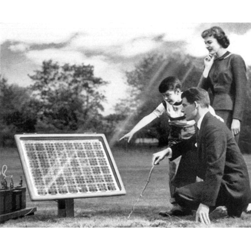
By the way, the ability to create p-n junctions also gave rise to photovoltaic cells, i.e. solar panels!
During this time, by accident, Bell Labs also discovered silicon dioxide’s protective and insulating properties:
In early 1955, Bell Labs researchers encountered a major problem with pitting on the surface of silicon wafers during high-temperature diffusion. This problem was overcome by chemist Carl Frosch during a serendipitous accident in which the hydrogen gas carrying impurities through the diffusion furnace briefly caught fire, introducing water vapor into the chamber. The resulting "wet-ambient" diffusion method had covered the silicon surface with a layer of glassy silicon-dioxide (SiO2). Developed further by Frosch and his technician Lincoln Derick in the ensuing months, this technique allowed semiconductor workers to seal and protect silicon wafers during the diffusion process (Source)
Another win for 1955! Plus, this oxide layer also enabled photolithography!
Researchers soon postulated that photolithography plus diffusion would enable the selective doping realistic needed to make smaller transistors on integrated circuits.
Check out Bell Labs’ 1957 photolithography patent filing, which specifically calls out transistor miniaturization:

In this patent, Bell Labs made a p-n-p germanium transistor with all three regions (emitter, base, and collector) integrated into a single germanium wafer.
We’re clearly on the way toward silicon-based integrated circuits! And with that, Moore’s Law.
1957 was also the year in which the infamous Fairchild Semiconductor came into existence, and they quickly made significant silicon transistor architecture and manufacturing improvements:
In just five months, the founders set up a crystal-growing operation (Sheldon Roberts), developed photolithographic masking techniques using 16 mm movie-camera lenses (Jay Last, Robert Noyce), established the aluminum characteristics needed for making electrical contacts (Moore), and built their own manufacturing and test equipment (Julius Blank, Victor Grinich, Eugene Kleiner) at their Palo Alto facility. Building on their exposure to Bell Labs techniques at Shockley, they developed the first commercial double-diffused (emitter and base) silicon mesa transistor, so named for its raised plateau-like structure. After successful delivery of the Moore team's n-p-n transistor, the device was introduced as type 2N697 to great acclaim at the Wescon trade show in August 1958. (Source)
Whew! They were busy. Here’s a 1958 advertisement, with a “visit us at Wescon” call to action at the bottom:

We’re not quite to integrated circuits yet though; this new mesa transistor met the performance needs of aerospace systems but had a major flaw; its exposed junctions made it vulnerable to contamination, limiting reliability.

Autonetics selected the device for a guidance-and-control system on the Minuteman ballistic missile, the largest defense program of the era. In late 1958 a potential reliability problem put the new firm's survival at stake. Tiny particles flaking off the inside of the metal package threatened to short across exposed junctions on the mesa structure.
Notice the “mesa” diagram above — a metal flake could short the base to emitter if it fell across them.
Fortunately, one of the “traitorous eight” Fairchild Semiconductor cofounders Jean Hoerni overcame the shorting issue with the invention of the planar proces which built on the previously mentioned silicon dioxide and photolithography innovations:
See the “planar” diagram — SiO2 can provide a barrier on the junctions, only exposing enough room for wires to make contacts with the junctions.
Seeking a solution to reliability issues with the mesa transistor, Fairchild physicist Jean Hoerni recalled an idea he had recorded in December 1957 - a new process in which the oxide layer is left in place on the silicon wafer to protect the sensitive p-n junctions underneath. Focused on getting its first devices into production, the company did not pursue the approach at that time. Due to concerns about possible contaminants, conventional wisdom required removing this layer after completion of oxide masking, thus exposing the junctions. Hoerni viewed the oxide instead as a possible solution - his "planar" approach, named after the flat topography of the finished device, would protect these junctions. After writing a patent disclosure in January 1959, he demonstrated a working planar transistor that March. The oxide layer was indeed found to protect the junctions, as Hoerni had predicted.
We’ve got the ingredients for integrated circuits!
In 1958, Jack Kilby of Texas Instruments demonstrated the first integrated circuit prototype; a simple oscillator built on a single germanium chip with transistors and passive components connected by wires.
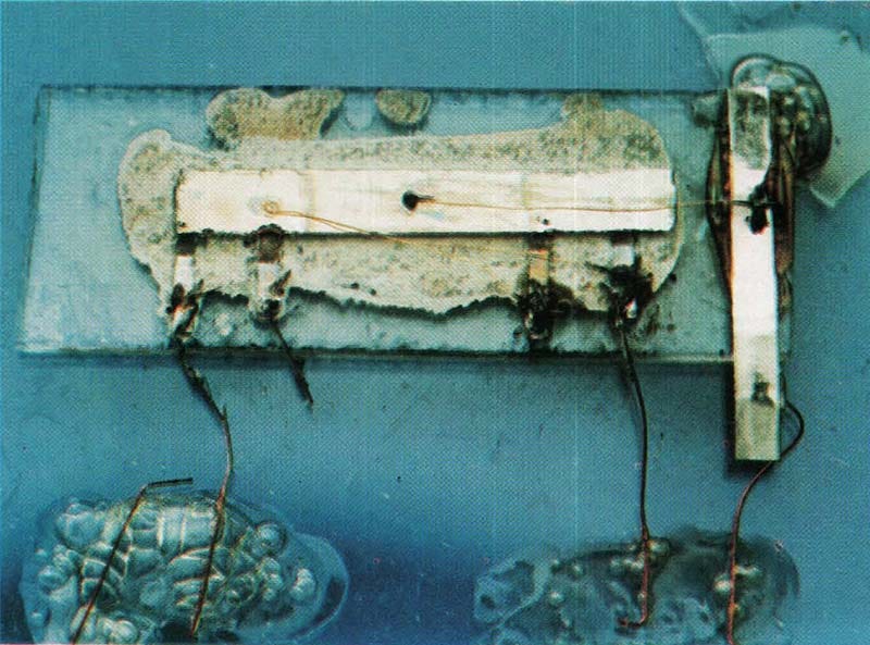
“Shown here is Kilby’s first IC, a phase shift oscillator. It’s made out of germanium (large rectangle) and contains a single junction transistor (under the aluminum bar in the center). The short perpendicular tabs are input and output terminals. The large vertical bar on the right is ground. Wires are made of gold and the entire device is held together with wax. It’s 0.062 inches long and 0.04 inches wide.” Source
This was the first time a circuit was fabricated in situ on a single substrate! Nevermind that it looks crude, these are lab prototypes.
And here’s a neat tidbit: in a July 1976 IEEE Transactions on Electron Devices paper, Kilby mentions that he graduated went to work for a company called Centralab after graduating from UIUC in ‘47. Centralab icensed the transistor from Bell Labs in 1952 and Kilby got to attend the aforementioned Bell Lab’s knowledge sharing symposiums!!!
It’s so fun to see the downstream impacts of Bell Labs’ inventions!
Back to Kilby’s IC — it was a great step forward, but used external interconnects that were handwired; not great for volume manufacturing.
In 1959, Robert Noyce at Fairchild Semiconductor used the planar process to fabricate multiple components directly on a single chip and introduced evaporated aluminum interconnects for on-chip wiring. I can’t find a picture of the 1959 IC, but below are some diagrams from the patent filed July 30th, 1959 (and granted in 1961). Pay attention to Figure 4, a side view showing how the P and N junctions are built into the silicon wafer:

And Figure 3 (below) is a top-down view that shows how each diode and transistor is isolated and connected by metal lines placed on top of an oxide layer.

Noyc'e’s key innovation was that both the devices and their wiring were made together on the same chip, eliminating the need for manually wiring separate components. Hence, Noyce’s design is more practical for mass production than Kilby’s hand-wired device.
And there we have it! An “integrated” circuit!
We’ve traversed from vacuum tubes, to discrete circuits, and now to integrated circuits.
The stage is almost set for decades of miniaturization that we call “Moore’s Law”!
Small Scale Integration
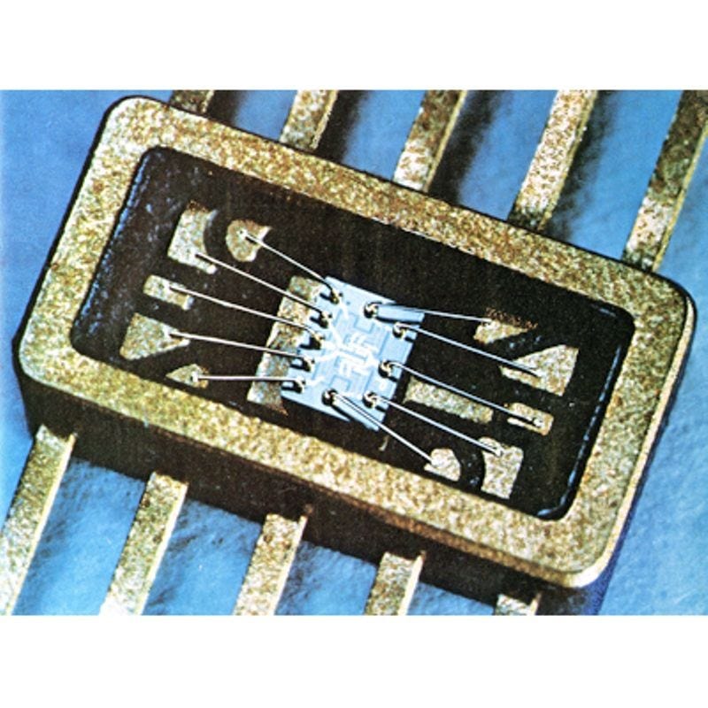
The early to mid 1960s was the integrated circuit era called “small scale integration” (SSI); the integrated circuits had say tens of transistors on a single chip. Not bad compared to that big 6 vacuum tube behemoth from IBM!
Below is a packaged Fairchild “G gate” integrated circuit used in the Apollo guidance computer (!!!) and manufactured by a company called Philco Ford:
I came across this awesome Fairchild ad from 1961 advertising their “silicon planar single chip circuits” (i.e. integrated circuits):

We went from large systems built via vacuum tubes, to large systems built with discrete transistors, and now systems were built from ICs with tens of transistor per chip.
Medium Scale Integration
How do we get to medium scale integration (MSI) of say hundreds of transistors on a single chip?
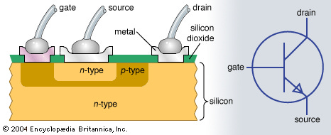
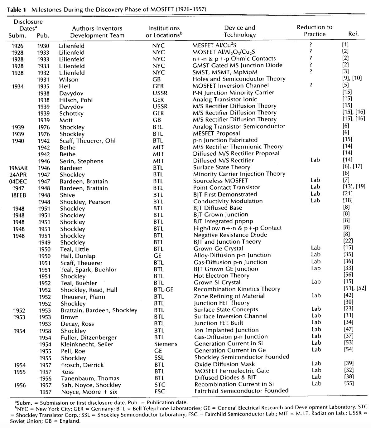
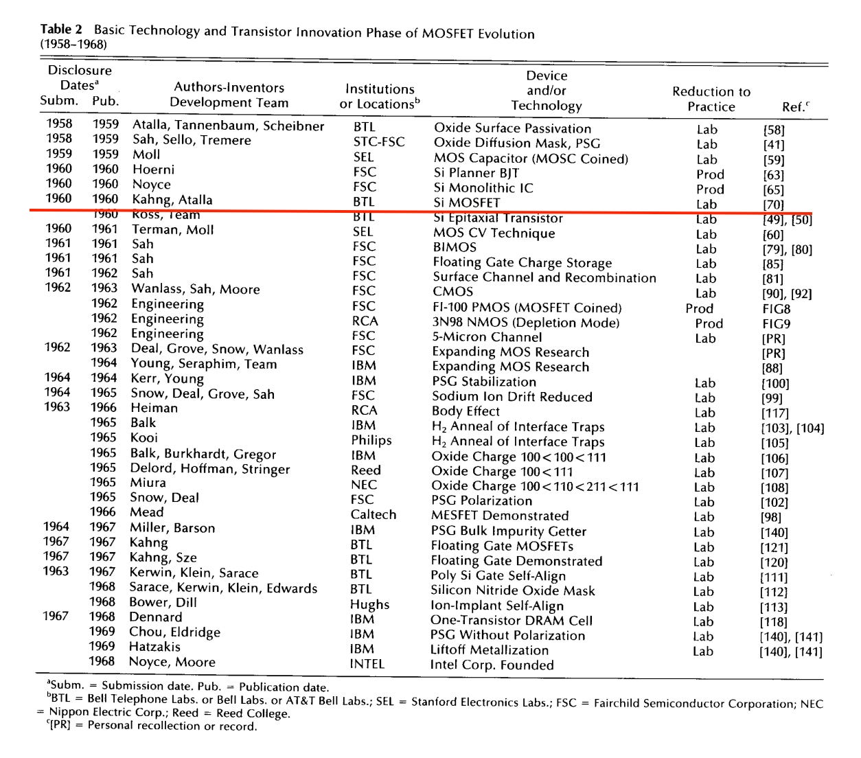
Noyce’s design used an emitter-base-collector design, also known as a Bipolar Junction Transistors (BJT). In hindsight, BJTs won’t unlock Dennard scaling and Moore’s law. We need MOSFETs!
As it turns out, during these same inventive years (~1959-1960), Bell Labs demonstrated and patented the silicon MOSFET transistor needed to unlock scaling! But they didn’t see it’s applicability for their telephone systems at the time so they shelved it. Yet, Bell Labs also noted it was easy to manufacture and could be useful for integrated circuits:
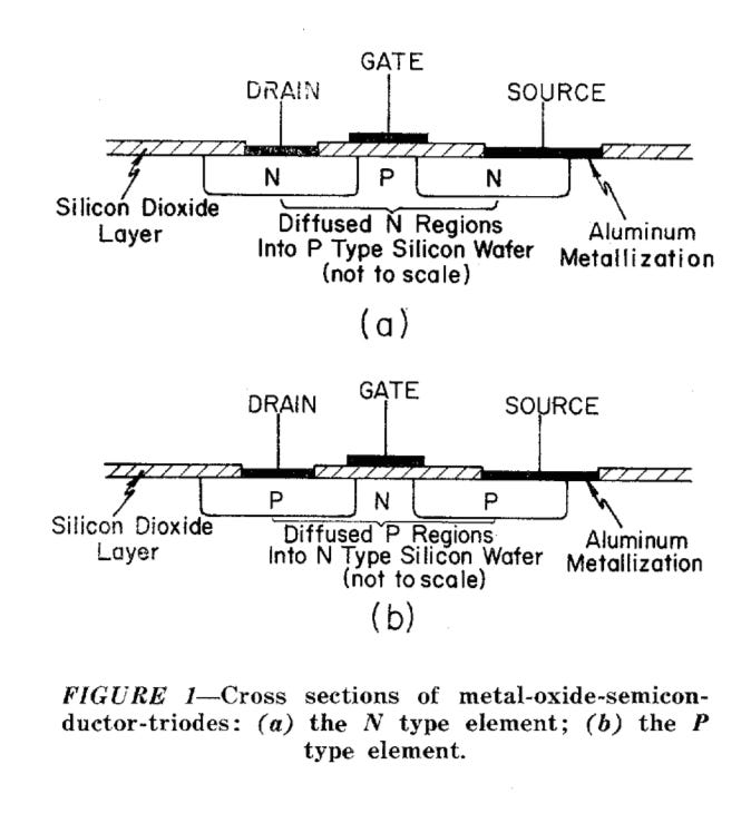
In 1959, M. M. (John) Atalla and Dawon Kahng at Bell Labs achieved the first successful insulated-gate field-effect transistor (FET), which had been long anticipated by Lilienfeld, Heil, Shockley and others by overcoming the “surface states” that blocked electric fields from penetrating into the semiconductor material.
Investigating thermally grown silicon-dioxide layers, they found these states could be markedly reduced at the interface between the silicon and its oxide in a sandwich comprising layers of metal (M, gate), oxide (O, insulation), and silicon (S, semiconductor)—thus the name MOSFET, popularly known as MOS. As their device was slow and addressed no pressing needs of the telephone system, it was not pursued further. In a 1961 memo, however, Kahng pointed out its potential “ease of fabrication and the possibility of application in integrated circuits.” Source
The idea of a field-effect transistor was a loooong time in the making, as recalled by Chih-Tang Sah who co-invented CMOS while at Fairchild in this 47-page magnum opus called Evolution of the MOS Transistor-From Conception to VLSI:
However, I want to reiterate two commonly held convictions: i) Recent inventions and new ideas have mostly come directly or indirectly from expanding and improving old ideas and previous knowledge. Even Lilienfeld’s 1926–1928 transistor inventions were probably influenced by his earlier (1920) and others’ experiences in vacuum tube research. The use of previous knowledge by a prepared mind was amply described and illustrated by Shockley in his descriptions of the invention of the bipolar junction transistor during 1947 [6]. ii) It was not enough just to have invented a new device or apparatus. It takes the ingenuity, persistency, and basic hard work of many dedicated engineers and technicians to put the inventors’ ideas into practice in order to produce inexpensive, high-performance and reliable integrated circuit chips, systems, and consumer products. In the limited space available, I cannot include the many reported and untold dedications, efforts, foresights, and interesting stories, but their importance in propelling the electronics industry to the present state of the art cannot be more recognized and appreciated.
And then Sah gave us this epic history of inventions that ultimately contributed to the MOSFET’s invention, which starts in 1926 and takes two pages to get to the Si MOSFET!
Whew. HOW’S THAT FOR DEEP RESEARCH, OPENAI!
Totally different topic, but it would be fun to see a historical lineage like this of all the related inventions that laid the groundwork for the Transformer neural network. Homework for the interested reader.
MOSFETs and CMOS
Well guess what. This same Sah co-invented the CMOS transistor and shared it in this 1963 conference paper titled “Nanowatt Logic Using Field-Effect Metal-Oxide Semiconductor Triodes”. Nanowatt should give you a hint how exciting this would be. In short, they demonstrated an arragement of p-channel and n-channel MOS transistors that consumes very little power when idle.
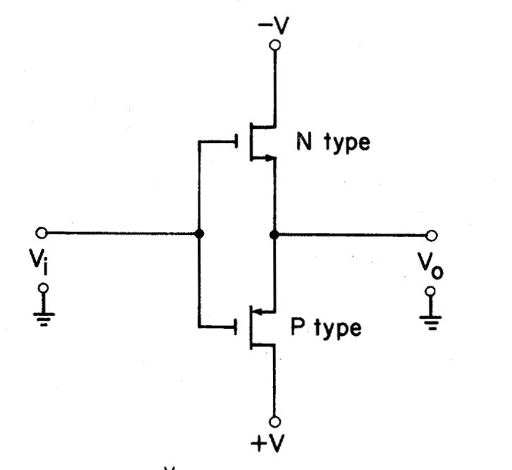
This complementary arrangement can be combined in straightforward manner to make logic gates!

Tada! NOR gates from CMOS.
Why is this important? NOR gates can be used to make any other logic gate like NOT, AND, OR, etc!

In the 1965’s RCA (Radio Corporation of America) made CMOS ICs for the government, and eventually made the CD4000 series of small-scale digital ICs using it’s 20 micron fabrication process (source).
But it took time for CMOS to catch on elsewhere.
LSI
Large-Scale Integration (LSI) time. By the way, you might have heard of company named LSI Logic. Jensen worked there for a bit!
Intel’s early processors focused on scaling existing PMOS or NMOS technology. For example, the Intel’s first microprocessor (the 4004) had ~2,300 PMOS transistors built with 10 micron process:

Thousands of transistors! That’s LSI!
By the late 1970s Intel launched the infamous 8086 CPU, this time with 3 μm nMOS and almost 30,000 transistors!

Transistor miniaturization was off to the races, with a march from 20 microns to 20 nanometers over the span of four decades.

VLSI
Somewhere in here we landed in the Very Large-Scale Integration (VLSI) era. For example, by the late 1980s, Intel’s 40486 launched with 1.2 million transistors! 486’s chief architect was Pat Gelsinger!
These CPUs were still packaged as a discrete chip. Here’s the package for the 40486, also known as the i486:
This discrete CPU was connected with other components like memory, graphics, and I/O chips via a printed circuit board. Here’s the entire motherboard for the i486:
Not how far we’ve come: from systems made of individual components (first vacuum tubes, then solid-state transistors) to systems made of individual chips (integrated circuits).
Yet, these printed circuit board circuits are bulky and power hungry. And those PCB metal traces slow down performance.
System-on-Chip
Fortunately, as transistor density improved it became possible to integrate entire subsystems onto a single chip; think CPU plus graphics plus memory on a single slab of silicon (a silicon “die”). This is the system-on-a-chip (SoC) era.
By 2017 Intel was up to 100 million transistors on a chip (source). You can put a lot of logic and related blocks on a chip when you’ve got a 100M transistor budget.
These “monolithic” SoCs have better power efficiency, performance, and area utilization compared to traditional multichip systems. Moreover, integrating all these components onto a single die gets rid of those external PCB communication traces, which lowers power consumption, reduces latency, and enables smaller product form factors (think smartphones, tablets, etc).
Apple’s M4 chip is a perfect illustration of a monolithic SoC:

Look at all of the CPU cores! There are four big performance CPU cores (“CPU1”) and six small efficient CPU cores (“CPU 2”). There’s also a 10-core GPU and 8-core Neural Engine (NPU).
That’s what’s possible with 28 billion (!) transistors on a single silicon die!
Downsides
Yet massive SoCs have trade-offs. They’re incredibly complex and design costs have skyrocketed; designing an SoC with diverse IP blocks (CPU, GPU, memory, analog, etc) requires signification design, integration, and validation effort. How do you know this thing even works?
Moreover, as transistor miniaturization below 10 nm is reaching it’s limits, manufacturing costs have exploded. This means SoC designers need serious volume to amortize these costs.
And notice that SoCs force every IP block to use the same process technology, e.g. 3nm. Yet not all blocks benefit from smaller transistors; analog and RF components may actually perform better on mature nodes like 28 nm or even 65 nm! Said mature nodes are significantly cheaper and have been optimized for a long time so they have better yields too.
Finally, as SoCs like Apple’s M4 chip grow in size, the manufacturing yield declines. A single defect anywhere on a large monolithic die can ruin the entire chip, and the bigger the die, the more likely a defect.
Oh yeah, physical limits like the maximum reticle (photo mask) size constrain how big a die can be; SoCs have a physical upper bound on size.
Chiplets
If transistors are hard to make smaller, and yet simply adding more cores to an SoC is hitting physical size limits… are we stuck? Is this long fun journey of scaling…. done?
Or can we overcome the limits of SoCs? Can we push back against those complexity, cost, and time-to-market trade-offs?
Stay tuned for the follow up article to understand how chiplets help the semiconductor industry continue building advanced systems that overcome these issues! We’ll of course discuss the trade-offs too.