

Understanding SkyWater
Deep Dive on $SKYT

If you like any of the following:
American semiconductor manufacturing
US national security
Rock’s Law
Berkshire Hathaway-style acquisitions
Quantum computing
Then you’re going to enjoy the story of SkyWater Technology, a pure-play semiconductor foundry in America’s heartland.

This will be a long and fun walk through the history and strategic choices that shaped the company, from why it exists at all to the specific playbook it’s using to grow.
First, to understand how SkyWater emerged, we need to rewind and look at the semiconductor industry's history that made its founding possible—nay, necessary. Then we can examine its differentiated strategy and future upside.
We start with the intersection of national defense and semiconductors.
Chapter 1: National Security and the Trusted Foundry Program
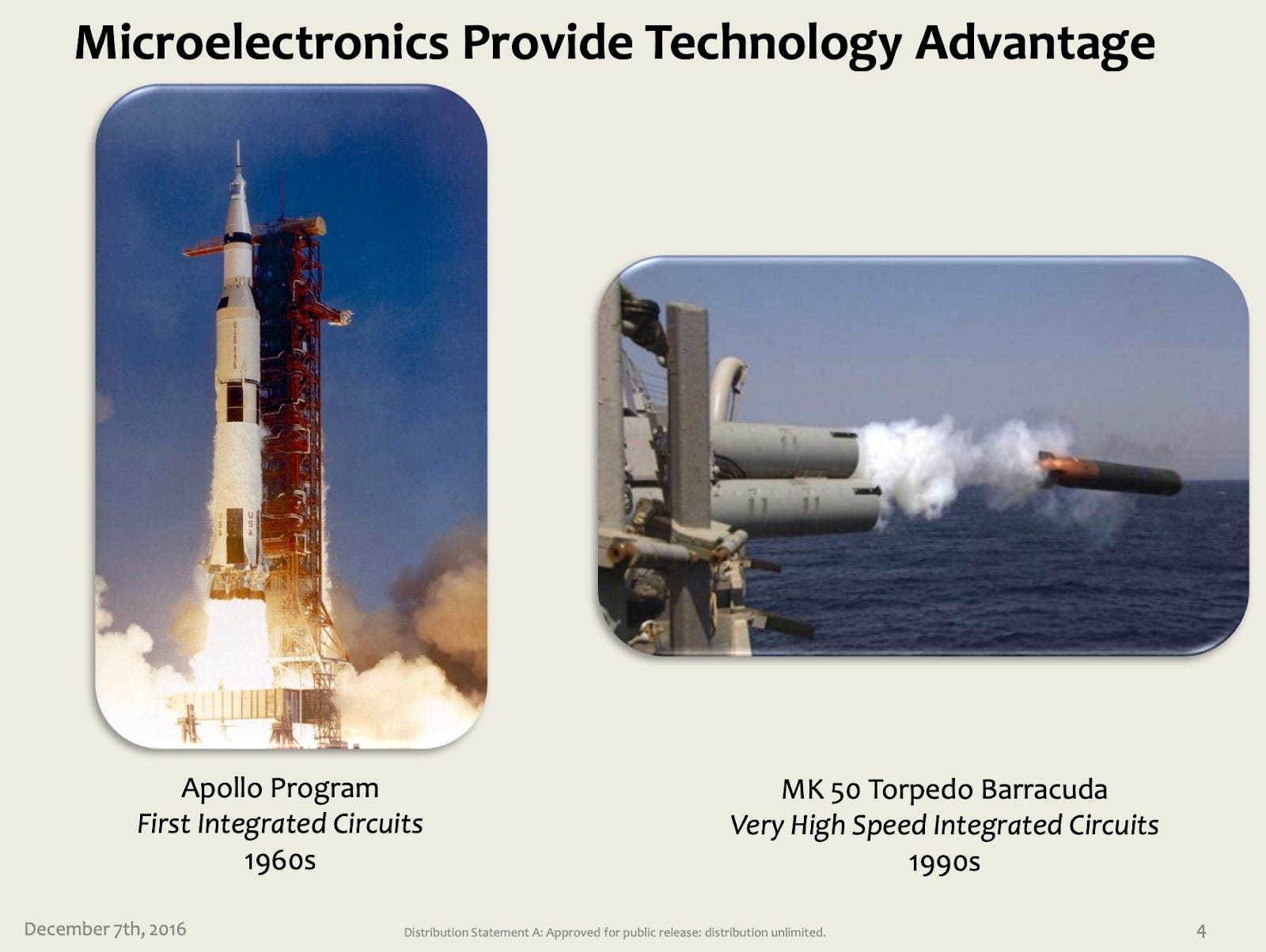
For decades, the United States has relied on the simple idea of deterrence through technological asymmetry; stay ahead by fielding technologies no rival can match.
Semiconductors have been the backbone of that strategy. They powered the guidance computers in Minuteman missiles in the 1960s, the radar and signal processors that made stealth aircraft viable in the 1980s, and the high-speed digital logic that enabled GPS-guided weapons in the 1990s.
In the early years, defense electronics were built by American integrated device manufacturers that designed and fabricated their own chips—think Fairchild and Texas Instruments.
Over time, however, manufacturing migrated overseas. First in assembly and test, then memory and logic, as pure-play foundries such as TSMC (1987) and UMC (1995) enabled the rise of fabless companies.
Rock’s law accelerated this shift:
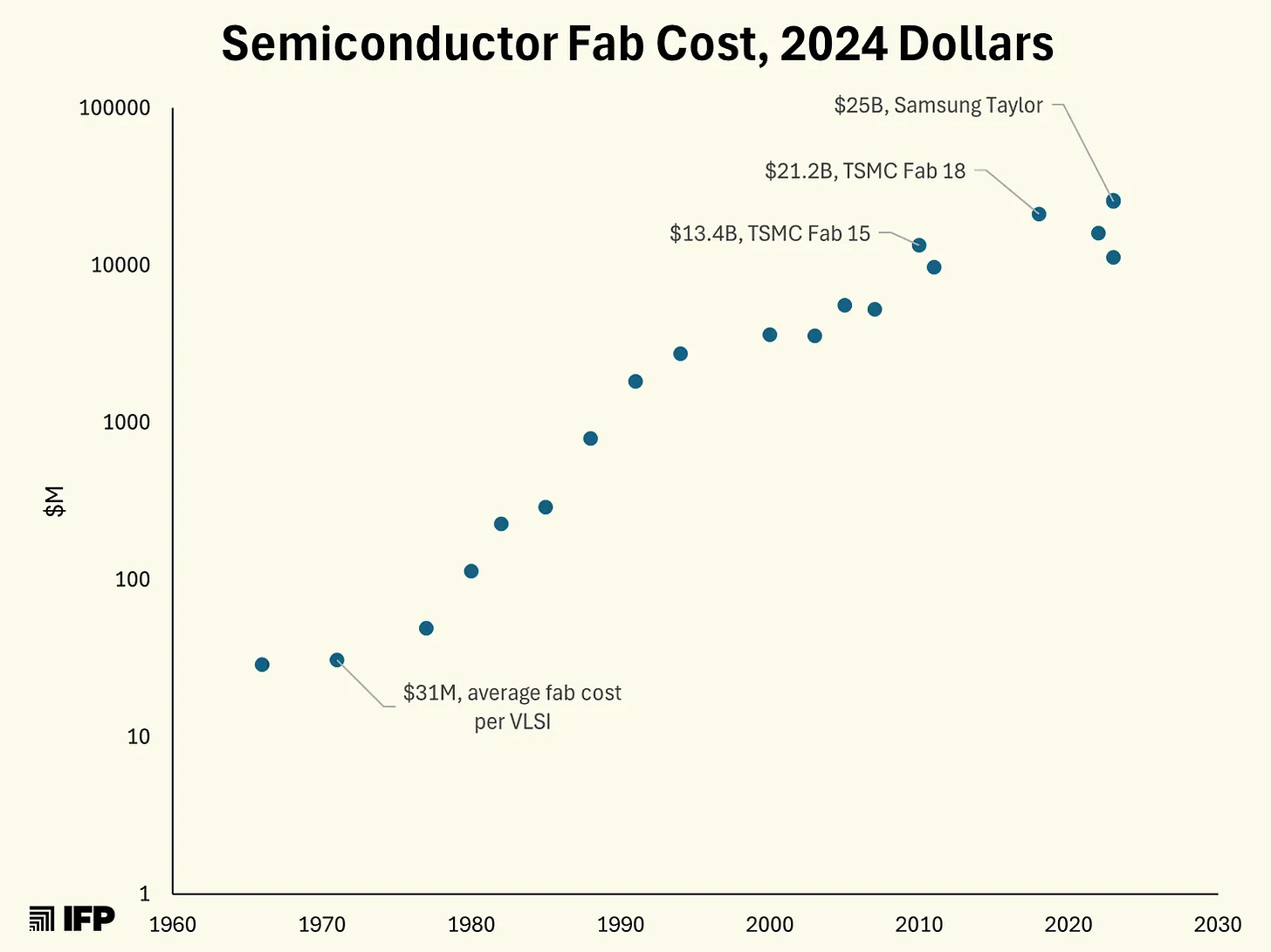
Don’t forget that chart, as it’s central to this story and much of semiconductor history.
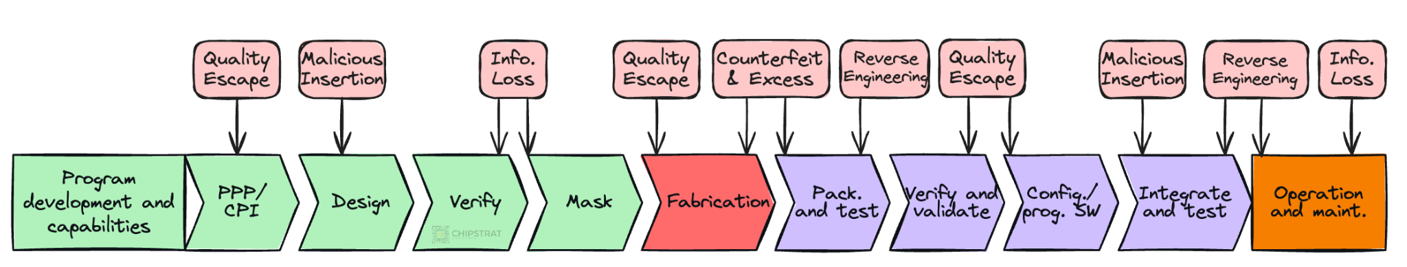
As economics and specialization pushed more of the supply chain overseas, it created openings for adversaries to tamper with hardware, extract IP, insert backdoors, and introduce counterfeits. Here’s an example of what can happen at various steps in the chip lifecycle:
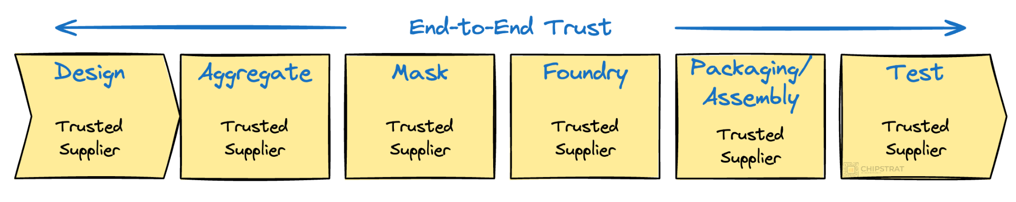
The Pentagon recognized the need for secure, on-shore production of the entire end-to-end supply chain.
That concern led to the Department of Defense and NSA launching the Trusted Foundry Program. Its goal was simple: ensure that the nation’s most sensitive chips could still be built, tested, and verified within U.S. borders.
The Trusted Foundry Program began as a long-term sole-source arrangement with IBM Microelectronics, which operated trusted fabs in Vermont and New York. At the time, these sites ran leading-edge nodes (90 nm and 65 nm). IBM also maintained specialized process technologies required for the most sensitive defense and intelligence systems, including rad-hard microelectronics and secure ASIC flows used in satellites, missiles, and classified platforms.
Although IBM was an integrated device manufacturer (IDM), e.g., manufacturing Power microprocessors, they also manufactured chips for other companies and alliances such as the PowerPC chips in Apple’s Power Macintosh lineup and the Cell processor in the PlayStation 3.
IBM has been in the semiconductor business primarily to supply leading edge technologies to its high-end systems and storage products. A portion of the manufacturing capacity is made available to supply commercial microelectronics customers with access to IBM’s advanced technologies, while improving IBM’s cost profile. Source
IBM functioned as a merchant foundry in this sense. Internal products took priority, but selling capacity helped keep the factories full.
Yet the government saw that relying solely on IBM’s leading-edge nodes left gaps in the end-to-end trusted microelectronics supply chain. By the mid-2000s, the program expanded into a broader Trusted Supplier framework, accrediting other companies along the supply chain to ensure end-to-end trust.
Even with that expansion, IBM remained the cornerstone. It was the only U.S.-owned merchant fab with leading-edge CMOS capability and DoD accreditation.
Good on IBM. The government doesn’t buy in huge volumes, but is a consistent buyer and a visible and important customer.
But… what if something happens to IBM’s fabs?
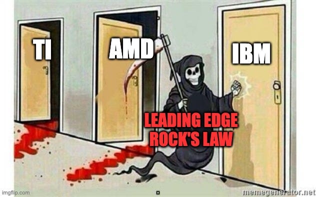
Chapter 2: Rock’s Law Reaper visits AMD, GlobalFoundries is Born
At the time, other IDMs ran captive leading-edge fabs, meaning the facilities existed solely to build chips for their own product lines rather than serve outside customers.
AMD is one such example. Although AMD is fabless now, there was a long history of AMD as an IDM. Most know this thanks to AMD founder Jerry Sanders’ infamous “Real men have fabs” quote.
I found a reference to the quote in the 1994 Bloomberg article Real Men Have Fabs. It’s a fantastic read and shows you how much the industry has changed since then!
Odd as it sounds, chipmaker Actel Corp. doesn’t make chips. It sells them, all right, and its designs for so-called programmable logic devices are hot. But the nine-year-old company farms out production to true chipmakers with spare capacity in their wafer-fabrication plants. This strategy was a winner for six years. Actel’s sales took off in 1988--and rose nearly 50% just in 1993’s first nine months. Then the downside of going “fabless” showed up. Manufacturing went awry at one of its foundries, and Actel couldn’t find a pinch-hitter. Some $3 million in expected fourth-quarter sales went down the drain, virtually wiping out profits.
Actel is hardly alone. “The fabs are full,” laments CEO John C. East. And that could signal the end of an era. It means that 250 fabless chip companies--the startup stars of Silicon Valley for a decade--face a growth crisis…
The fabless wonders have thrived by exploiting a capacity glut, mainly in Japan. There, memory-chip makers expanded greatly in the early 1980s--just before demand waned. Many of those fabs were at 60% of capacity as recently as 1992, according to consultant VLSI Research Inc. By using them, U.S. entrepreneurs avoided the main hurdle for a chip startup: the tens or hundreds of millions in wafer-fab costs. A new venture could thus devote its resources to innovative designs, such as faster clones of Intel Corp.’s microprocessors or multimedia chips that vastly improve graphics on personal computers. By pioneering these cutting-edge products, fabless companies grew faster and earned higher returns than established chipmakers--giving them clout way beyond their 5% share of the $77 billion world chip market.
Now, everything is changing. The boom in advanced PCs crammed with memory chips, coupled with stingy capital spending in Japan, is boosting utilization of Japan’s older fabs to 80% or more. Worse, surplus capacity in the most modern fabs--those that print circuit-line widths of 0.8 micron or less--has shriveled to 3%, says VLSI Research. That’s bad news because the designs of the fabless folks usually require advanced production processes. Says G. Dan Hutcheson, VLSI’s president: “All the conditions that made fabless companies possible are coming to a close.”
…
Years ago, as the fabless trend picked up steam, Advanced Micro Devices Inc. Chairman W.J. “Jerry” Sanders III was skeptical. “Real men have fabs,” he growled. Now, many fabless companies concede his point. “Silicon [production] is no longer ‘free,’” says Barry L. Cox, president of fabless Weitek Corp. So Cox and his counterparts are hastily devising survival strategies. One is simply to avoid designing chips that demand the latest manufacturing processes, thus avoiding fabs where capacity is tightest. That can’t work for long, though.
Sanders made this infamous statement back in the early 1980s, when the cost of a new fab was “only” $50-100M.
But fabs are dominated by fixed costs. You pay for the cleanroom, tool depreciation, facilities, and engineering staff whether you run one wafer or 100,000. Variable costs are small in comparison.
As nodes advanced, fab complexity and capital cost climbed into the multibillion-dollar range. Those larger fixed costs had to be spread across many more wafers. If wafer output did not rise, the fixed cost per wafer rose, pushing up a company’s chip costs.
AMD had enough volume to fill its fabs in the 1970s and 1980s. By 2007, a multibillion-dollar fab required volumes AMD could no longer support.
Rock’s Law Reaper came knocking:
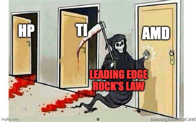
Time to go fabless.
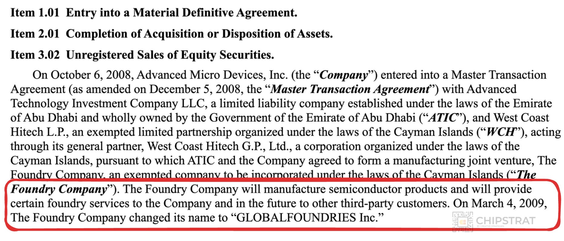
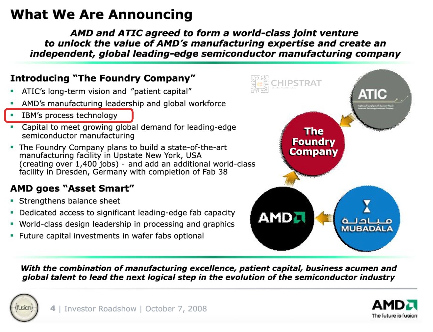
As this Oct 2008 AMD Investor update shows, AMD made the decision to spin its fab into a new joint venture called The Foundry Company (which was later renamed GlobalFoundries):
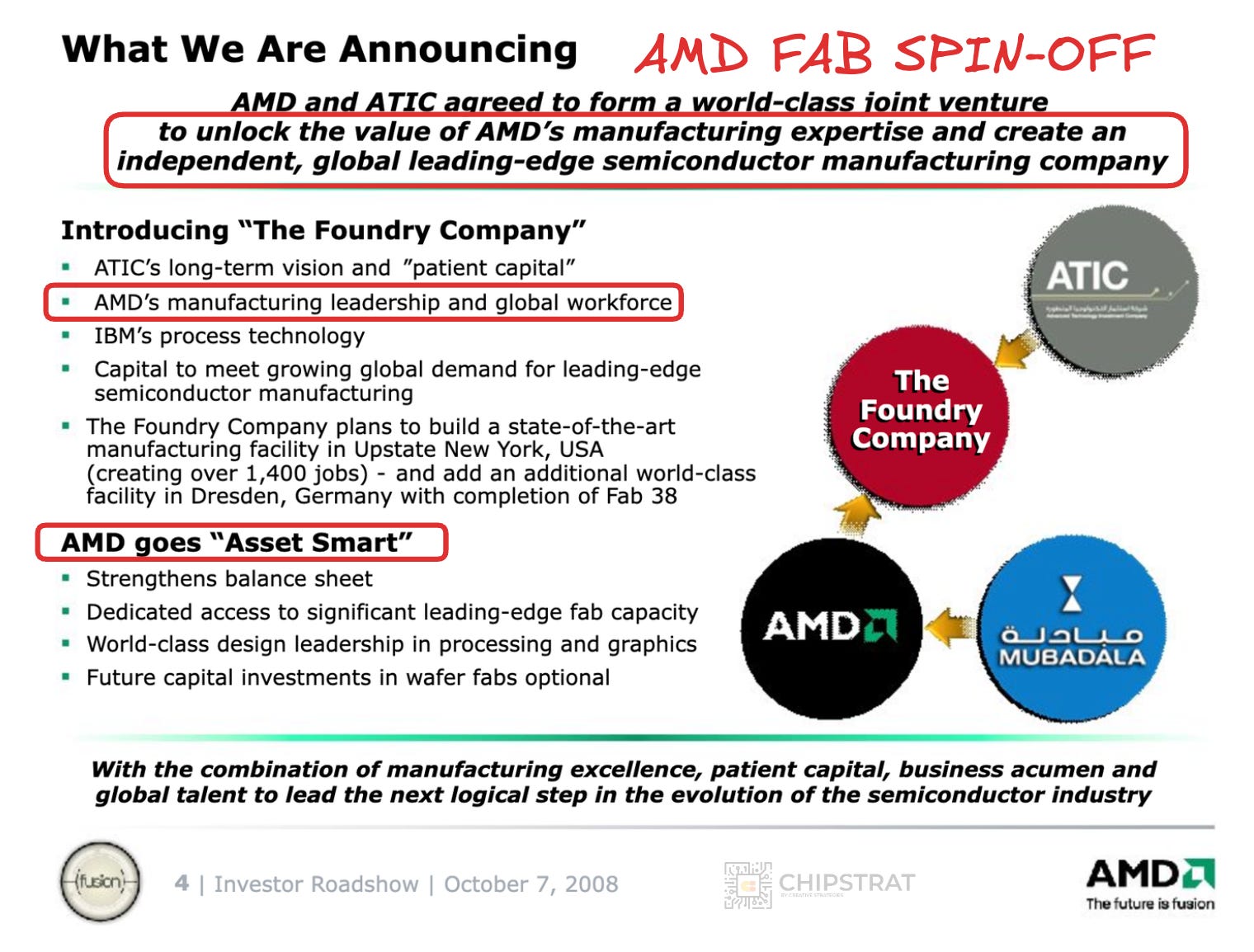
“The Foundry Company” was majority owned and managed by a holding company ATIC that was wholly owned by the Government of Abu Dhabi:
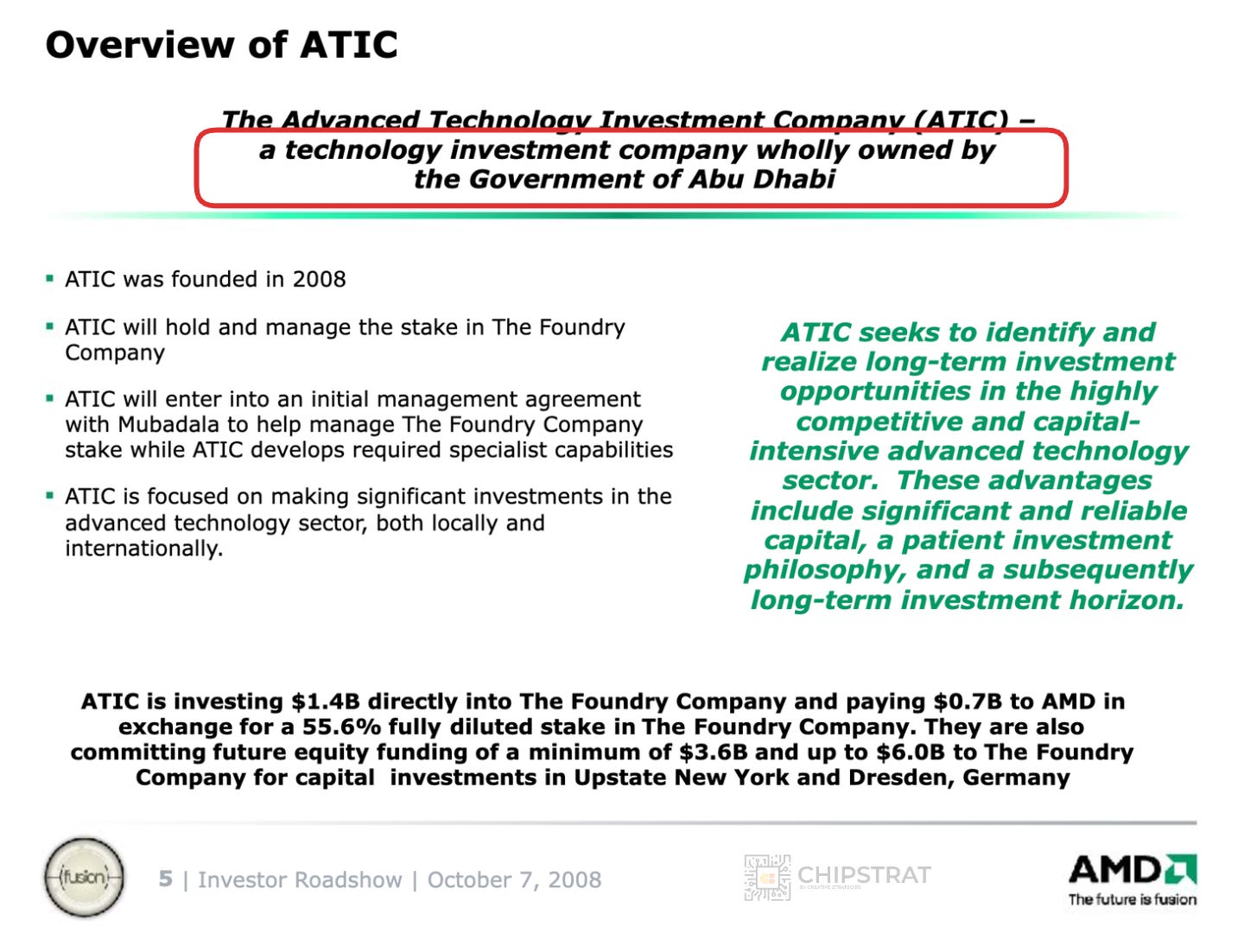
The Government of Abu Dhabi, through ATIC and via Mubadala, held 55.6 percent of The Foundry Company and was set to increase its stake over time unless AMD matched future capital investments. (Which, of course, they wouldn’t, because they wanted out of that CapEx game). Five months later The Foundry company was officially launched as GLOBALFOUNDRIES:

GLOBALFOUNDRIES. All caps. Why are we yelling?
They toned it down from all caps to camel case in 2019 😃
So here we see that GlobalFoundries is majority-owned by a foreign government.
Take that in.
This will create up an opening in the market in the near future…
We’ll get there in a minute, but first we need to take note of a very important lesson from the AMD fab reckoning: AMD sold its fabs for a loss.
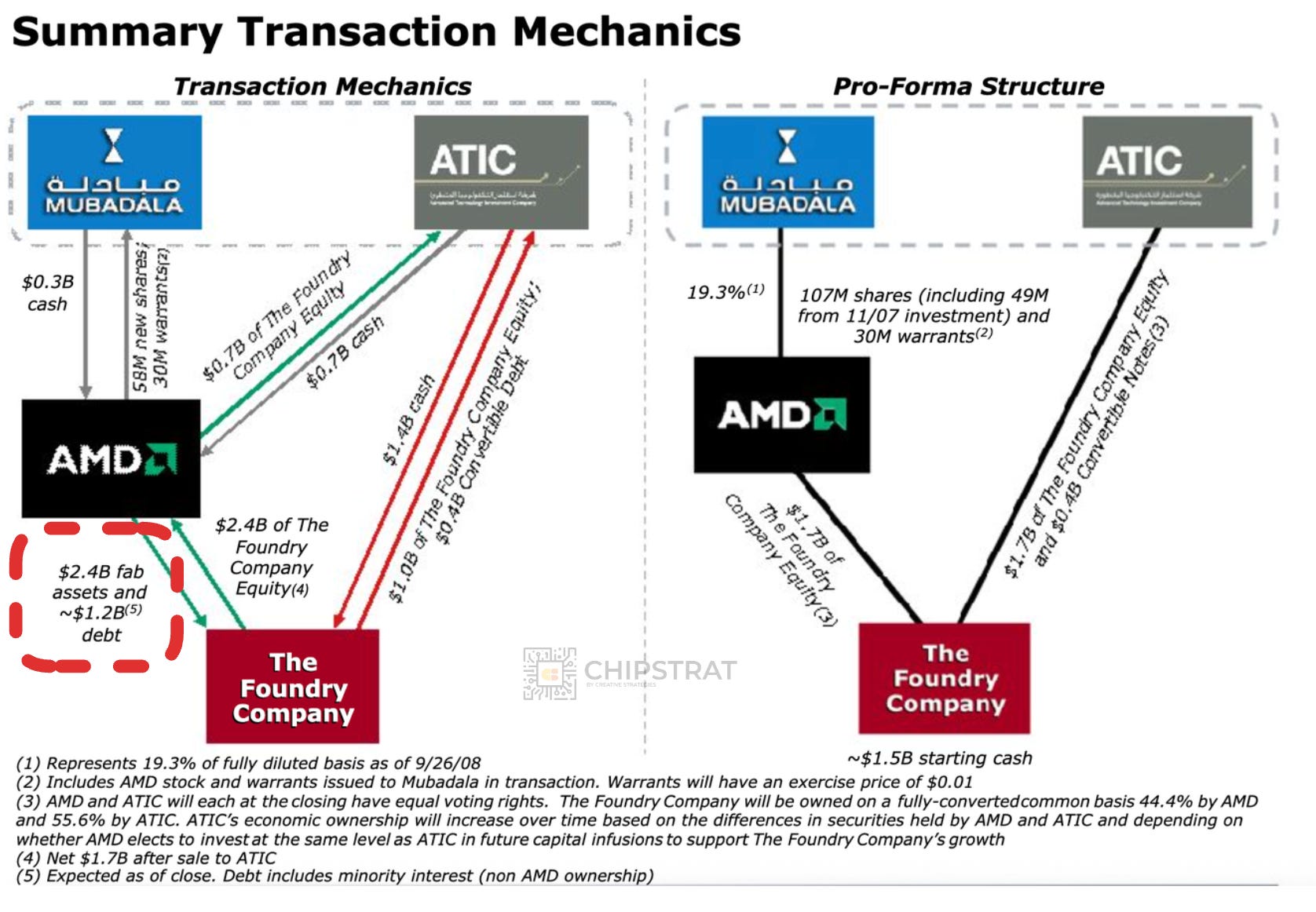
AMD divested $1.2B of assets (manufacturing assets and IP, plus people) to The Foundry company (GlobalFoundries). In return, it received a minority stake of the joint venture and $700M of cash.
Willing to sell dollars of assets for dimes to divest of the fab…
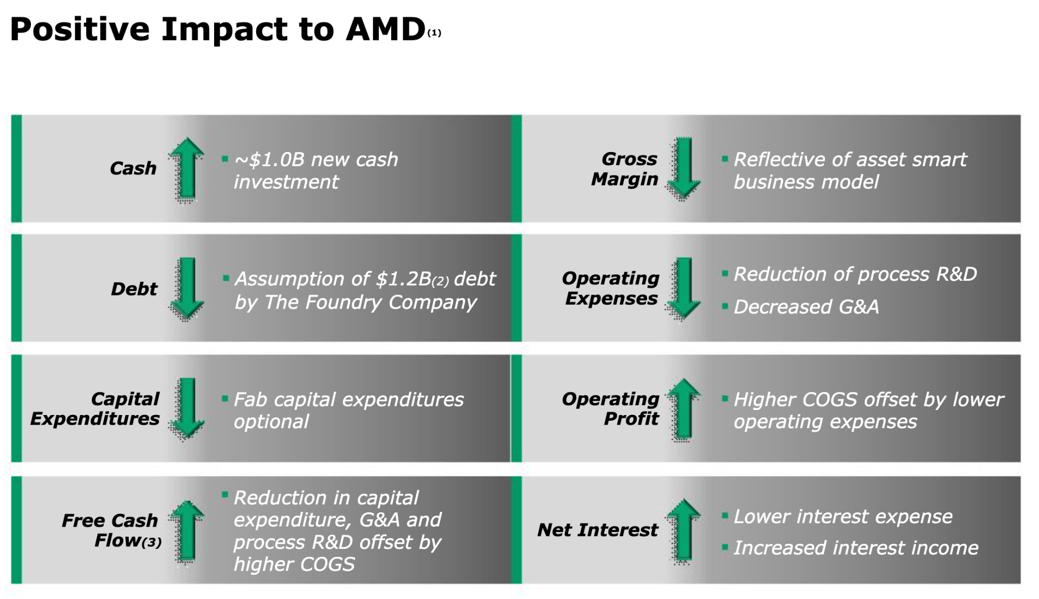
Still, AMD’s shedding of its fab was the right move. It left AMD with less debt, more cash, and far lower capital requirements:
There was a time when Jerry Sanders could be gutsy and continue playing the game, but those days were long gone. AMD humbly knew now was the right time to walk away:

But why would anyone take the other side of this deal? How the heck would the joint venture keep the fab full?
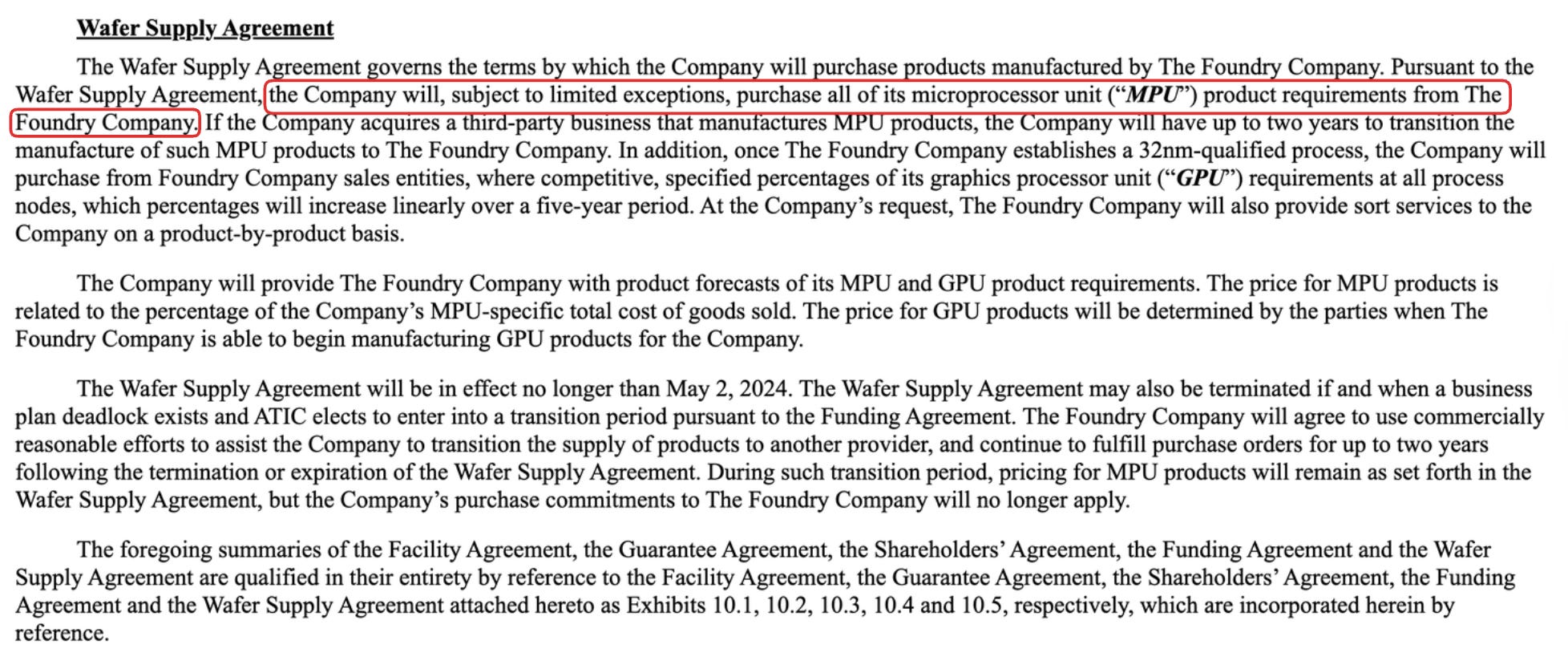
For starters, the joint venture agreed to a long-term wafer supply agreement.
AMD agreed to use GF exclusively for leading-edge CPU production through the 32 nm and 28 nm generations:
What in the world does any of this have to do with SkyWater?
Just tuck this lesson in your cap for now: companies looking to shed their foundry are happy to give it away for dimes on the dollar and pair the sale with a multiyear wafer supply agreement. That keeps the fab somewhat loaded while the buyer finds new customers to increase utilization and diversify the revenue mix.
Spoiler alert: the deal unraveled because of the leading-edge race.
The deal structure itself was fine, but Rock’s Law Reaper was still in hot pursuit, only now aimed at a brand-new company carrying the burden":

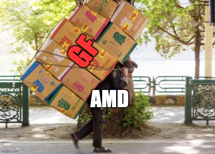
AMD wasn’t off scot-free either. A struggling GF became a serious drag on AMD through the wafer-supply exclusivity agreement:
Fast-forward a bit: GlobalFoundries fell behind on 32 nm, 28 nm, and 14 nm nodes, so AMD had to repeatedly amended its wafer agreement to unwind the exclusivity, which cost nearly $1 billion in penalties.
Now, as we’ll see later.. that fab spinoff model actually can work, but with trailing edge fabs. Sell the fab and lock in a wafer-supply deal, as long as the buyer is taking on trailing-edge capacity. No Reaper to fend off.
By the way, you may have noticed in the AMD foundry spinout slides, Mudabala also received a significant amount of stocks and warrants for $300M cash infusion it gave AMD.
AMD will sell to Mubadala 58M new shares and 30M warrants(1) in exchange $0.3B which will increase Mubadala’s ownership in AMD to 19.3% on a fully diluted basis
For the next several years, Mubadala was the largest AMD shareholder!
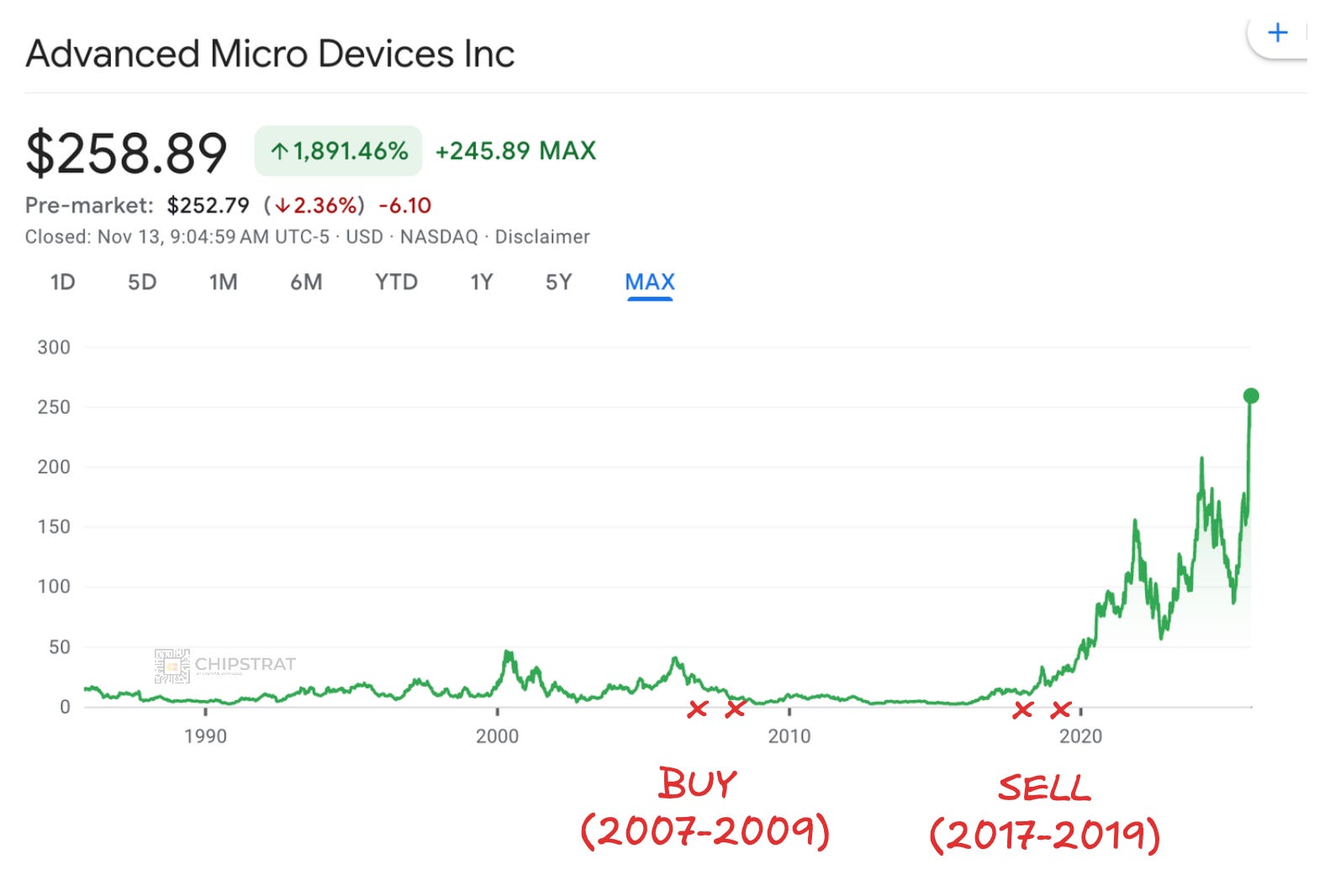
But Mubadala started unwinding those shares from 2017 to 2019 😬 Mubadala definitely made money, as they exited during the $10 to $30 move, which looked good then. Of course, with the stock now above $250, they obviously missed out on the AI trade 😅
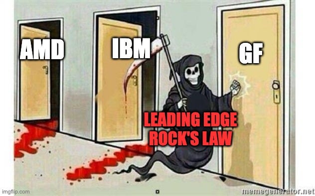
The reaper moved on from AMD. GF was able to keep it away for a period of time, but IBM Microelectronics was struggling, and the government’s secure supply would soon be at risk…
Chapter 3: The Reaper Comes for IBM
By 2014, IBM could no longer afford the cost of leading-edge fabs, as it didn’t have enough internal and external volume to keep them profitably utilized.
In the divestiture announcement, IBM made the strategic rationale explicit:
While IBM has world-class technology and intellectual property, the company has lacked scale. As a subscale business, IBM’s Microelectronics business has been generating losses. The technology manufacturing process will become more complex as the node progresses from 22nm to 14nm and then to 10nm and even more challenging for a subscale operation. This progression will entail incremental manufacturing capacity and re-tooling to support increasing development effort and more challenging chip yields.
Subscale business, and the losses are mounting.
Who might be interested in buying IBM’s fabs?
Why, GlobalFoundries of course!
On October 20, 2014, IBM and GLOBALFOUNDRIES announced that they have signed a Definitive Agreement under which GLOBALFOUNDRIES plans to acquire IBM’s global commercial semiconductor technology business, including intellectual property, world-class technologists and technologies related to IBM’s Microelectronics business.
There are two important takeaways here.
First, we see GlobalFoundries picking up another fab as a distressed asset.
GF was already intimately familiar with IBM’s process technology.
Did you catch that AMD was licensing IBM process technology reference in the AMD spinout slides?
A 2004 EETimes article describes the relationship,
For the past decade, Advanced Micro Devices Inc. has been searching for a way to achieve parity with Intel Corp. in process performance. In just the past year, to reach that goal, the chip maker has turned from a partnership deal with Motorola to one with UMC and, now, from UMC to IBM’s microelectronics division.
Analysts said the deal with IBM to co-develop processes at the 65-nm and 45-nm node gives AMD a good chance to catch up with Intel in transistor performance and to introduce the process at approximately the same time as its larger competitor.
About 50 AMD process development engineers will work with IBM technologists at IBM’s Semiconductor Research and Development Center in East Fishkill, N.Y. The project begins later this month, with the goal of having the jointly developed 65-nm process ready for possible joint 300-mm manufacturing in late 2005.
Here we see the lengths to which AMD went to keep the Reaper at bay. Their own process R&D was slipping, so they tried to anchor themselves to any partner that could help them keep pace. This existing relationship obviously gave GF familiarity and confidence in the IBM R&D team.
While that AMD IBM relationship helped GF with diligence, the real driver was the economics of building a new foundry business. A fab is mostly a balance sheet full of expensive tools. Buying a used fab is often the cheapest way to acquire those tools, and acquiring a foundry also means inheriting its book of business. In IBM’s case this means IBM’s wafer needs plus a set of external fabless customers.
And the sellers usually make the deal irresistible. Remember,
companies looking to shed their foundry are happy to give it away for dimes on the dollar and pair the sale with a multiyear wafer supply agreement
Like AMD before it, IBM sold foundry assets on the cheap and committed to a wafer agreement with GF:
IBM and GLOBALFOUNDRIES have signed the Agreement under which GLOBALFOUNDRIES will acquire IBM’s semiconductor manufacturing operations and facilities in East Fishkill, NY, and Essex Junction, VT and its commercial microelectronics business. GLOBALFOUNDRIES will become IBM’s exclusive server processor semiconductor technology provider for 22nm, 14nm and 10nm semiconductors for the next 10 years.
One interesting anecdote is that IBM paid GF $1.5B for the privilege of walking away from its fab business. IBM also took a $4.7B write-down.
IBM will reflect a pre-tax charge of $4.7 billion in its financial results for the third quarter of 2014 related to the divestiture of the Microelectronics business. This pretax charge includes impairment of long-lived assets to reflect the fair value less the estimated costs of divesting the Microelectronics business, which the company classified as held for sale at September 30, 2014, cash consideration of $1.5 billion and other related costs. The cash consideration of $1.5 billion is expected to be paid to GLOBALFOUNDRIES over the next 3 years, and will be adjusted down by the amount of working capital which is estimated to be $0.2 billion.
Why would GF absorb a money-losing manufacturing division even with IBM paying to hand it over? Because the deal delivered two assets GF needed.
First, it gained IBM’s leading-edge process R&D team, the same engineers who had co-developed advanced nodes with AMD. AMD was GF’s largest logic customer, and GF needed that technical depth to keep AMD competitive as Intel pushed down the roadmap.
Second, it diversified GF’s portfolio. IBM contributed Trusted Foundry technologies and customers. Those programs had steady demand and were insulated from the financial brutality of the leading-edge node race, giving GF a more durable revenue base and a buffer from the economics that had already strained both AMD and IBM.
Spoiler alert: This diversification became extremely important for GF when The Reaper came calling just four years later (2018):
Chapter 4: The Opportunity
Back to 2014 when IBM sold its fabs to GR.
There’s one obviously big problem with IBM divesting its fab as you’ve surely noted.
America’s “trusted foundry” was no longer American-owned.
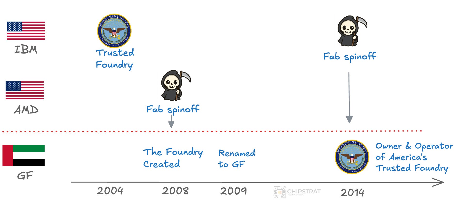
The UAE owned Mubadala. Mubadala owned GlobalFoundries. And now, GlobalFoundries owned and operated America’s Trusted Foundry.
The government accreditation stayed with the fabs, so the capability stayed in place on American soil, but there was obviously now supply chain risk given the foreign ownership.
Policymakers saw it immediately. From the House of Representatives’ Committee on Armed Services report in May 2016:
The committee remains concerned with the Department of Defense’s ability to ensure access to cutting-edge microelectronics with the requisite level of verifiable trust incorporated. The committee recognizes that the Department’s ability to provide superior capabilities to the warfighter is dependent, in part, on its ability to incorporate rapidly evolving, leading-edge microelectronic devices into its defense systems, while also balancing national security concerns. Currently, the Department processes for ensuring trust rely on assessing the integrity of the people and processes used to design, generate, manufacture, and distribute national security critical microelectronics. For over a decade, the Department has relied on a single domestic source for trusted leading edge microelectronics…
The committee understands that one of the trusted foundries capable of producing strategic-hardened microelectronics for the Department of Defense was sold to a foreign-owned company in 2015. In testimony before the committee on October 28, 2015, the Acting Deputy Assistant Secretary of Defense for Manufacturing and Industrial Base Policy expressed concern about the dwindling number of domestic microelectronic manufacturers. In the committee report (H. Rept. 114-102) accompanying the National Defense Authorization Act for Fiscal Year 2016, the committee noted that the acquisition of the microelectronics fabrication and related intellectual property by a foreign-owned entity creates uncertainty about the Department’s future access to strategic-hardened trusted microelectronics and presents risk for the national security programs that rely on these products.
That’s a really serious problem.
Looks like a really good opportunity.
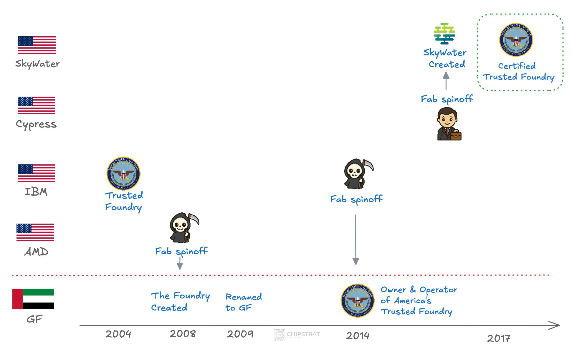
Chapter 5: SkyWater is Founded
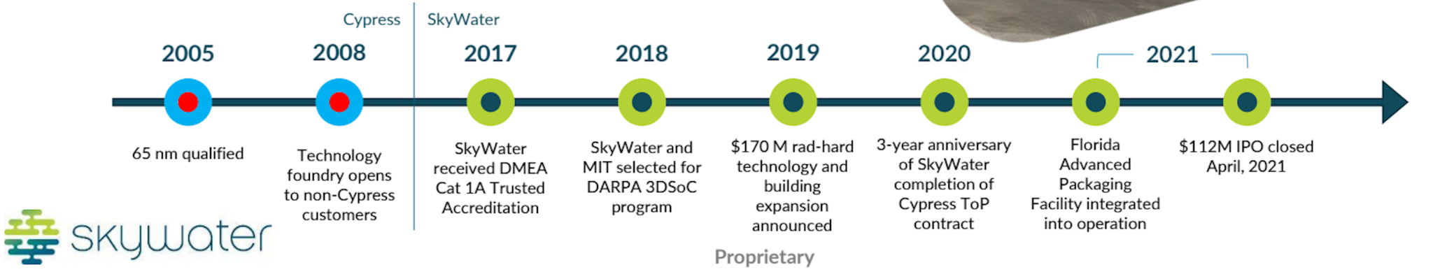
In March 2017, SkyWater was founded, kickstarted by a fab spinoff from Cypress Semiconductor.
(Cypress was later acquired by Infineon, a German company, in 2020.)
Notice that it wasn’t Rock’s Law Reaper this time, but simply a business decision.
Cypress’ press release from Mar 1, 2017 captures the story well. I’ll break it into chunks and explain:
Cypress Semiconductor Corp. today announced it has sold the subsidiary that owns its semiconductor wafer fabrication facility in Bloomington, Minnesota to SkyWater Technology Foundry for $30 million.
Cypress had a wholly owned subsidiary called Cypress Minnesota Inc running it’s Bloomington MN fab. This subsidiary traces back to a 1991 fab spinoff from Control Data Corporation.
Cypress Semiconductor Corp has stepped forward as the surprise buyer for what is left of Control Data Corp’s VTC Inc chip unit. VTC’s bipolar operations went in a management buyout in October and CDC thought at that time that it would simply have to close the Minneapolis-based CMOS operation. Cypress is paying a total of $14.7m for the VTC Class-1 semiconductor wafer fab and it reckons it got an out-and-out bargain. “We bought a $26.5m semiconductor facility, land and some equipment for $11.5m and have also agreed to buy leased manufacturing equipment which costs $32m for just $3.2m paid in stages over the next two years”, said Cypress chief TJ Rodgers. The $60m VTC facility will be run as an independent subsidiary, known as Cypress Minnesota Inc. Control Data also agreed to incur up to $4.6m of the new company’s operating costs during the first two quarters of 1991, ensuring that the acquisition will have no impact on Cypress’ profit and loss statements before the third quarter, by which time the operation should be profitable. Source
Hey look, a distressed asset sale with the seller even paying some of the buyers costs (and presumably some sort of wafer agreement). A tale as old as time!
This is a playbook if I’ve ever seen one!
And you might remember CDC was the company where Seymour Cray designed the CDC 6600, the first machine labeled a supercomputer.
Ok, back to Cypress and SkyWater.
Who is this SkyWater, and where did it’s $30M to acquire Cypress Minnesota come from?
Backed by Minnesota-based holding company Oxbow Industries, LLC, SkyWater Technology has purchased the capital stock of the subsidiary
So Skywater’s initial funding came from a private equity firm called Oxbow Industries.
SkyWater … will operate the fab as a standalone business that will manufacture wafers for Cypress and for other semiconductor manufacturers.
Here we see a clear articulation of Skywater’s strategy. Use the fab to
Make wafers for Cypress
Make wafers for others
Cypress was an IDM but couldn’t run this fab at full capacity. Not good. A fab carries heavy fixed expenses for tools, facilities, and engineering whether it runs at 10 percent or 90 percent. If volume drops, those fixed costs get spread over fewer wafers, raising cost per wafer and squeezing margins.
So they were willing to sell it to SkyWater; given that SkyWater is a foundry, they can go find other customers to increase utilization (“fill the fab”) and improve unit economics. There’s the playbook again!
The press release continues:
The transaction allows Cypress to reduce its manufacturing footprint and cost structure while increasing the utilization of its Fab 25 in Austin, Texas, in line with the company’s plan to improve gross margins.
Yep. Sell the fab, shift some of the wafers to Austin to increase utilization there, and buy the rest from SkyWater. That should improve gross margins.
Take note of Fab 25 in Austin, as it comes back into the story many years later….
Cypress CEO Hassane El-Khoury reaffirmed this is just a good business decision (and not Rock’s Law Reaper).
“This transaction demonstrates our commitment to reshape Cypress and improve gross margin, in line with our long-term financial model,” said Hassane El-Khoury, Cypress President and CEO. “The sale of Fab 4 in Minnesota allows us to reduce our manufacturing costs as we exit the fab while using the proceeds to pay down debt. We will also be able to improve the utilization and efficiency of Fab 25 in Texas, into which we have been transitioning products over the last 18 months. We believe this agreement represents another milestone in our path to achieving higher gross margins.
An incredibly important step when acquiring a fab is retaining the employees who have all the tacit knowledge needed to keep the manufacturing process running smoothly. This is important for both the buyer (SkyWater) and the seller (Cypress).
“In addition to looking at a potential deal’s impact on Cypress’ bottom line, we set out to ensure uninterrupted supply for our customers,” continued El-Khoury. “This agreement allows Cypress to maintain uninterrupted wafer supply for our products manufactured at the fab, with no disruptions for our customers, and it gives our former employees in Minnesota the opportunity to help the new business flourish and continue the fab’s tradition of quality U.S.-based manufacturing.“
This Minnesota fab is a 200mm fab at 90nm+ geometries. Hmm. That would be good for military use cases right?
“Given the proven history of efficiency at Fab 4, the expertise and dedication of its workforce and its established success in delivering specialized wafers on time to a diverse customer base, the SkyWater management team sees a strong foundation for growing a standalone business,“ said Dr. Scott Nelson, Chief Technology Officer of SkyWater Technology Foundry. “We are committed to continuing the fab’s support of Cypress and its customers with superior quality and on-time delivery.”
Obviously, SkyWater needs to meet Cypress’ needs, and also wants to fill the fab with other customers.
Wouldn’t it be great for a new foundry to get some stable defense customers?
Chapter 6: SkyWater Becomes a Trusted Foundry
Just 19 days after that Cypress press release, SkyWater made the following announcement: SkyWater Technology Foundry Achieves Cat1A Trusted Foundry Accreditation from U.S. Department of Defense
SkyWater Technology Foundry today announced that its production scale microelectronics wafer fabrication facility in Bloomington, Minnesota has been Accredited by the Defense Microelectronics Activity, a branch of the U.S. Department of Defense (DoD) as a Category 1A Trusted Foundry.
This accreditation enables SkyWater Technology Foundry to provide wafer fabrication, design, wafer test, and broker services as a Trusted Supplier.
“The fact that this was accomplished within two weeks of the birth of the company demonstrates the priority SkyWater Technology Foundry has put on this Accreditation and in serving the needs of the DoD,” said Michael Moore, Executive Vice President of Sales and Marketing. “This Accreditation validates our security posture and it demonstrates the continued commitment of this site to serving the microelectronics needs of the U.S. DoD.”
Boom.
The release continues:
The business plan for SkyWater Technology Foundry incorporates the ability to address the growing call for U.S.-owned and U.S.-based suppliers of microelectronics at a time when more and more of the microelectronics supply chain is migrating to China and other Far East countries.
“SkyWater Technology Foundry plans to expand engagements with the U.S. DoD generally, and in particular is poised to meet the requirements of DoD Instruction 5200.44 which requires fabrication of mission-critical custom microelectronics components in a Trusted facility,” he said.
Brilliant. Buy a fab, fill it partially with a wafer agreement with the seller, and use the spare capacity to meet the needs of the DoD at a time when there was no other US-owned trusted supplier.
I love that last sentence of the announcement too, which I read as: oh yeah, don’t forget you’re *required* to build in a Trusted facility… that’s us. Or you can pick foreign-owned GF. Your choice.
Here’s where we’re at in the story:
Chapter 7: Hiring a CEO
Running a pure-play trailing-edge American foundry is not an easy job. Finding the right CEO isn’t easy either.
Defense customers expect U.S. leadership, which narrows the field to a small number of Americans with true pure-play foundry experience.
And this person need to have a creative business plan. The government is not a huge customer; there are only so many satellites and missiles etc. Drones might eventually increase silicon content by an order of magnitude… but at this point we’re still in 2017, pre-Ukraine.
The Minnesota fab runs low volume, roughly 10K to 50K wafers per month depending on mask complexity. Cypress provided an anchor customer, but that still created concentration risk. The new CEO needs to get more customers ASAP; having existing industry relationships would be a huge benefit.
And while SkyWater avoided the leading-edge Reaper, trailing-edge economics bring their own pressures, particularly rising competition from China on foundational nodes. For those unawares, Chris Miller’s “Foundational Chips: China’s Ambitions and Implications for the U.S. Manufacturing Base” statement to the House Select Committee on the CCP explains:
Chinese [trailing edge] firms receiving vast state funding or benefiting from state ownership don’t operate according to market principles. If they produce uneconomic volumes and sell below market prices, they will put pressure on Western semiconductor firms’ profitability. Most problematic, they will deter new chipmaking investments in the West. This is already impacting the calculus of Western chipmakers and their investors.
The CEO must understand how to differentiate against this.
And finally, producing wafers is a capital-intensive process with low margins. As a startup foundry, they’ll have to get clever with financing because they’re not going to fund growth with cash.
So who might understand (and not be afraid of) all these dynamics? And have creative strategy and financing plans to boot?
In Oct 2017, SkyWater announced that Thomas Sonderman fit the bill:
… Sonderman was vice president of manufacturing technology at GLOBALFOUNDRIES. Formed as a spin-off of AMD’s manufacturing operations in 2009, GLOBALFOUNDRIES is a $4.0B full-service semiconductor foundry serving more than 150 integrated circuit customers worldwide. A key contributor to the spin-off, Sonderman assumed global responsibility for utilizing proprietary Design for Manufacturing and Automated Precision Manufacturing technologies to create a competitive advantage for the company. During his tenure, he built and led a team that transformed AMD’s manufacturing operation into an independent manufacturing powerhouse able to effectively compete with competitors ten times its size.
“I’m very excited to join SkyWater,” said Sonderman. “Our company has a differentiated foundry portfolio and a highly motivated team. I look forward to leveraging my experience at GLOBALFOUNDRIES to create a truly world class technology foundry that delivers tremendous value over time.”
Nice! Sonderman had lived this playbook! He spent 11 years at AMD, moved with the manufacturing team into the GF spin-out, and was a key contributor to the three-year process that created GlobalFoundries. Hard to find more relevant experience!
Of course, he had his work cut out for him:
Sonderman’s immediate focus will be on defining new product markets and target customers while simultaneously driving operational efficiencies.
Ah yes. Brass tacks. As CEO, Sonderman needs to figure out how to sustain and grow this business.
Chapter 8: Business Model Innovation
Sonderman’s most important task was defining a viable business model for SkyWater.
The classic pure-play foundry model is built for high-volume, standardized CMOS. It works when a company invests billions in a leading-edge node, publishes a fixed PDK, and earns its return by running massive, predictable wafer volumes for customers like Apple, Nvidia, AMD, Qualcomm, etc. Fixed costs stay efficient only when the fab is consistently full.
None of that applied to SkyWater. Bloomington was a 200 mm foundational-node fab with modest output, and Cypress was essentially the entire revenue base. Any dip in Cypress volume would hit SkyWater’s P&L directly. The cash cycle made it worse. A wafer-only model collects little up front and pays out only when finished wafers ship, which is brutal for a newly independent foundry.
SkyWater needed a different approach that stabilized revenue, reduced dependency on a single IDM, and created a path to economic viability without the scale that supports traditional foundries.
Hmmm….
So what differentiators could SkyWater leverage to power a viable business model?
The Bloomington fab came with an unusual asset: a process-development capability embedded in the same environment that produced commercial wafers. The fab could run research-oriented process work and production manufacturing side by side. Similar to how Intel’s Oregon sites pair process R&D with pilot lines.
Cypress needed that model as a mid-sized IDM building mixed-signal and embedded products that required custom device technology and nonstandard process tweaks.
To its credit, Cypress recognized a business opportunity: it began selling access to both R&D and manufacturing to external customers that needed custom process work. Startups in MEMS, photonics, quantum, and other nonstandard technologies needed process engineering help and a fab willing to co-develop, qualify, and scale their devices without forcing a site transfer when moving to production. Cypress called this it’s Specialty Foundry.
Skywater acquired this capability (and people), and also the Specialty Foundry customers:
As part of the assignment, which closed October 2, SkyWater will now have direct responsibility for all Specialty Foundry Business customers, eliminating the prior Cypress interface. Because of the existing working relationship between all parties, there will be a seamless transition for all current projects; the same team will continue working with all existing customers, the only difference being that they are now SkyWater employees.
SkyWater took that foundation and built a business model around technology development as a core offering. Customers come with early concepts, SkyWater’s engineers help turn those concepts into manufacturable flows, and the same fab can then scale production.
SkyWater calls this business model innovation “Technology as a Service” (TaaS).
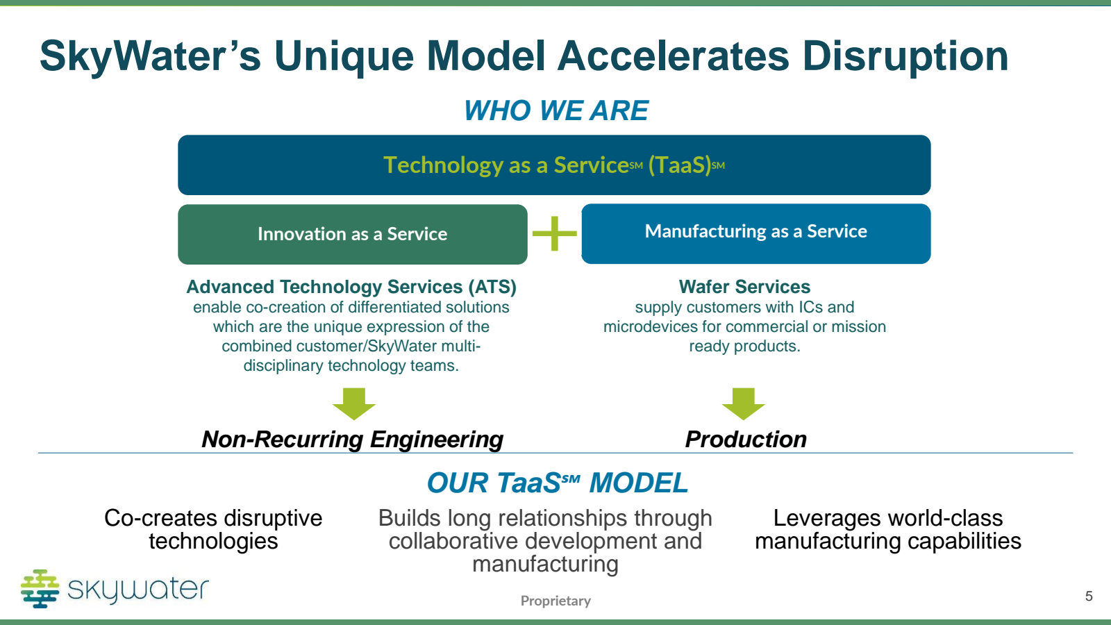
As you can see, this adds up-front NRE revenue for the R&D support in addition to wafer revenue as the chips are taped out.
Think of this sort of like Arm’s business model, where Arm receives licensing fees up front and then royalties as chips tape out. Similarly, Skywater gets revenue up front as R&D and also makes money over time via wafers.
That NRE money is higher margin for SkyWater than wafers too.
With this approach, SkyWater can fill a gap in the market:
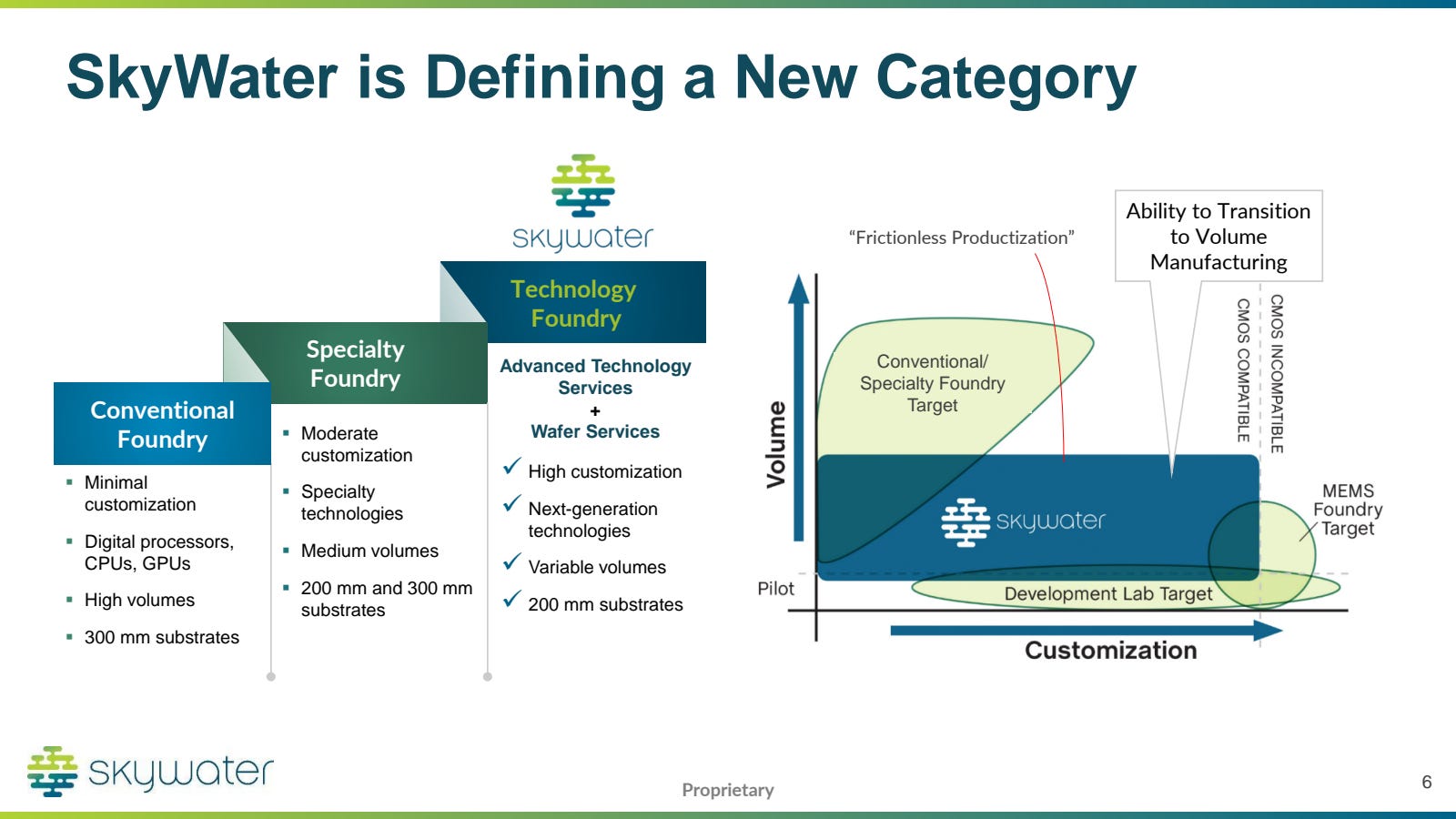
Traditional foundries generally won’t touch high-customization work. Research labs do, but can’t deliver production wafers.
SkyWater sits in the middle. It can take early R&D concepts, develop the process, and then run the same technology in a production-grade, trusted fab. This lets customers build complex or unconventional devices without owning a fab themselves and also speeds up time to market compared to working with several foundries:
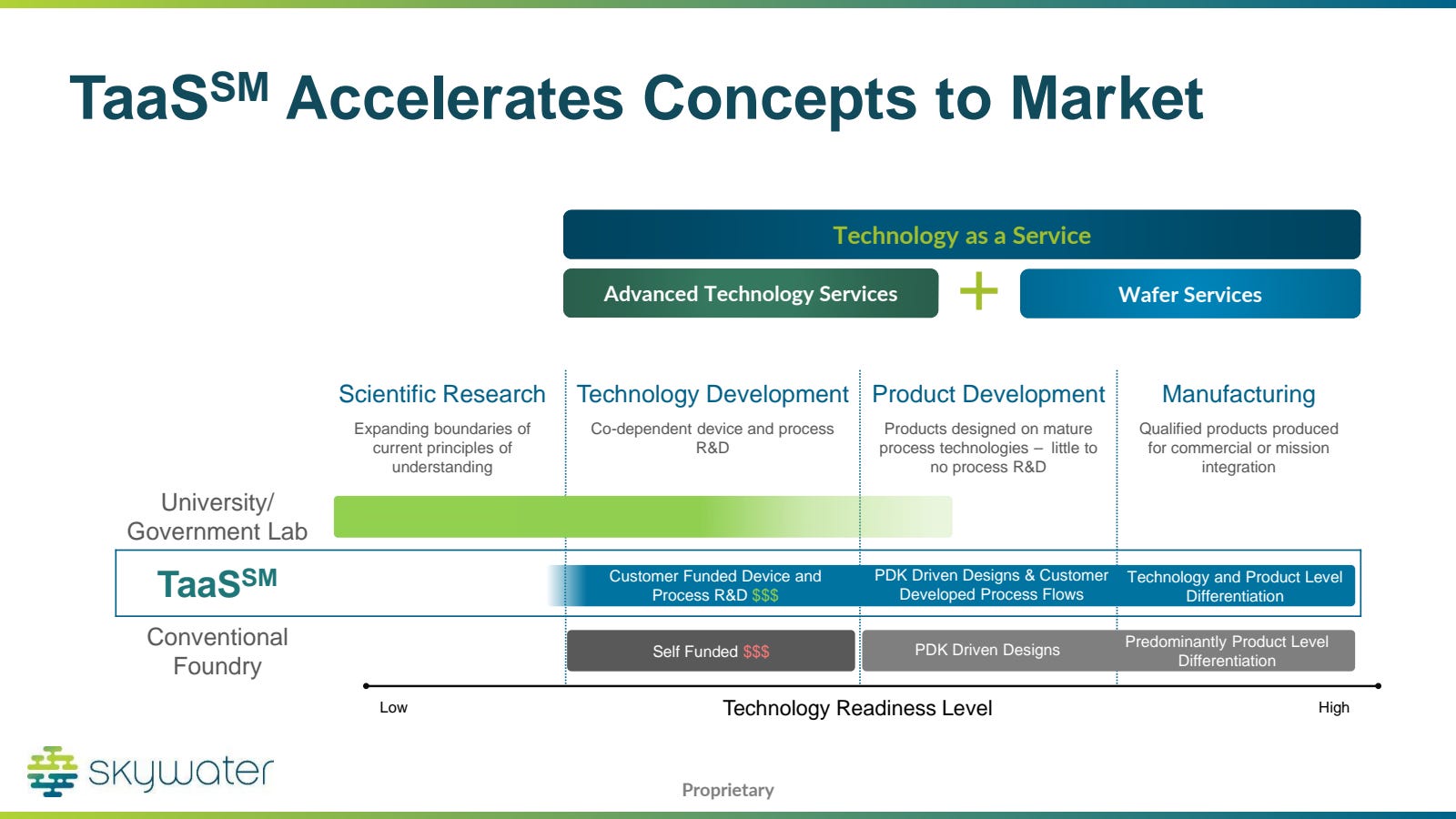
SkyWater describes itself as a virtual IDM. Customers get process development, device co-design, secure manufacturing, and a path to volume, without the capital or operational burden of running a fab.
And it turns out there was pent-up demand for this value prop, especially from Trusted Foundry customers. From a recent (and great) podcast with Skywater CEO Tom Sonderman:
TS: So we had an advanced 200 mm fab that was running volume production but also had a capability, a foundational capability to do R&D. That allowed us to tap into certainly the DoD market. There was a lot of pent-up demand. If you recall, GlobalFoundries had just acquired IBM’s microelectronics business. IBM had been a primary supplier to the defense industrial base, and so we came into the scene at that time. Of course, GlobalFoundries at the time was not a public company and was owned 100% by the government of Abu Dhabi. And so having a pure play foundry but also 100% US investor-owned capability allowed us to capture the attention of the DoD, and that brought in some programs that really got SkyWater on the map and allowed us to demonstrate this ability to do development in a high-volume manufacturing environment.
By the time of its S1 filing (to go public) in March 2021, Skywater’s business model had proven to be working:
We have reduced our revenue concentration from Cypress/Infineon to approximately 29% of our revenues for the year ended January 3, 2021 from approximately 100% of our revenues from the period of acquisition to July 1, 2017. As of January 3, 2021, since divesting from Cypress in March 2017, we have added four new customers to our Wafer Services business and 21 new customers to our Advanced Technology Services business
Chapter 9: Running The Playbook + Advanced Packaging
Skywater’s 2021 S1 revealed another interesting strategic decision: Skywater would add advanced packaging (AP) capabilities.
AP is a broadly important trend, but is also means Skywater can be the trusted partner for packaging.
As our industry evolves into a post-Moore’s Law reality, we believe 2.5D, 3D, and SiP advanced packaging concepts will be adopted broadly and our domestic offering for development and manufacturing of solutions in this space will be in high demand. Furthermore, our strategy is to make these services available not only to our customers developing highly differentiated and disruptive front-end technologies but also to advanced packaging services that may source chips from other foundries and seek our support for onshore heterogeneous integration solutions. In addition, as interest grows within the federal government to enhance domestic infrastructure in this area, we feel we are well-positioned to lead efforts to position the U.S. as a leader in advanced packaging technology.
How might Skywater develop advanced packaging muscles? The S1 hinted at it:
Expand our capabilities through cost-effective capital management, including seeking M&A opportunities to drive growth. We will continue to invest in additional manufacturing capacity and evaluate growth opportunities through acquisitions of other businesses and operations, including, with respect to (1) other foundries, (2) larger foundries looking to divest existing low-volume programs, (3) low-cost manufacturing capacity that increases our scale and (4) adjacent markets such as advanced packaging, or AP, and bond/assembly/test, or BAT. We also may expand our current facility or convert existing spaces into clean rooms to add to our contaminant-free manufacturing environment. We believe acquiring low-cost U.S.-based facilities will expand our scale and customer base while maintaining our domestic competitive advantage without disrupting current operations.
Acquisition?
Yep. Skywater picked up an Advanced Packaging Facility in Florida.
It was yet another Warren Buffet-style acquisition of an underperforming asset bought at a discount:
TS: When we got engaged with Osceola County, they had built a facility that had a false start. We came in, became the operator, and now in partnership with Osceola County, we’ve not only executed on some existing programs that that they had kicked off before we got involved, but we brought in another program, again, another DoD-funded program to stand up a wafer fan-out level packaging technology that again today exists only in Asia, bring that to the US. It’s on 300 mm, so this is our first move into 300 mm.
Three months later, SkyWater raised $112M in an April 2021 IPO. Here’s the updated timeline so far:
Chapter 10: Running The Playbook Again For More Volume
But what happens if Skywater gets super successful with ATS? Imagine many of the ATS customers are successful and need to ramp to decent wafer volumes. Could Minnesota become oversubscribed?
That’s not a concern anymore!
Remember the Cypress press release that mentioned Fab 25 in Austin TX?
Well, Cypress became Infineon… and Infineon eventually decided to sell Fab 25.
To SkyWater, of course.
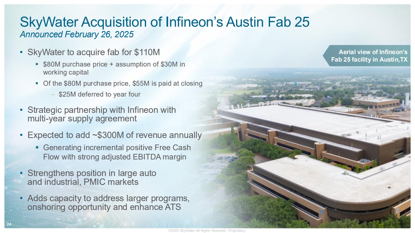
From June 2025:
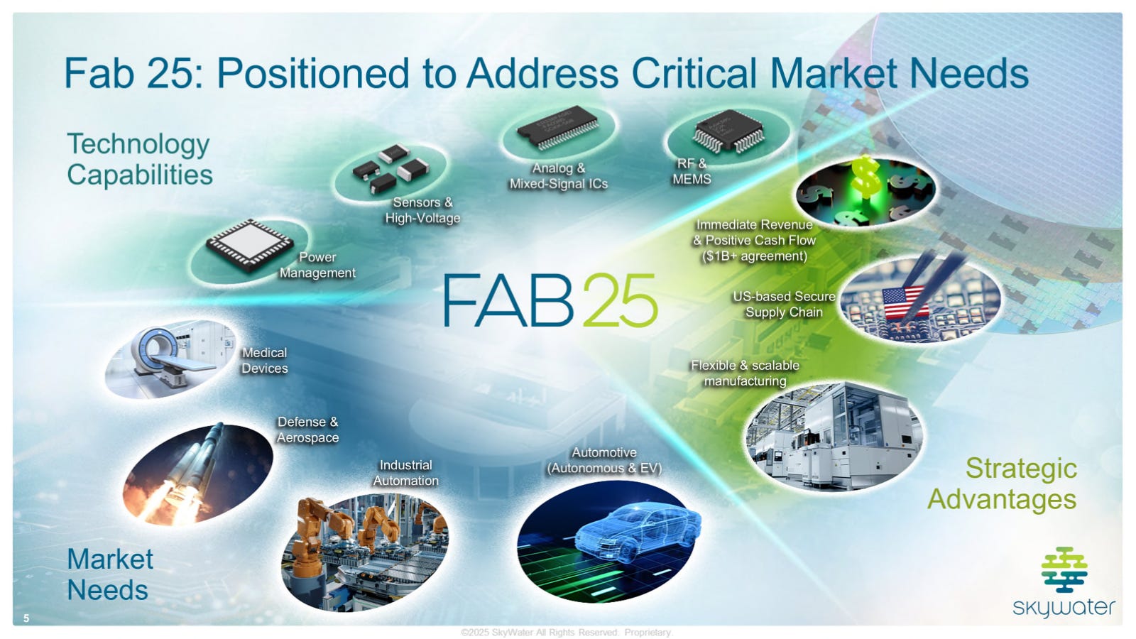
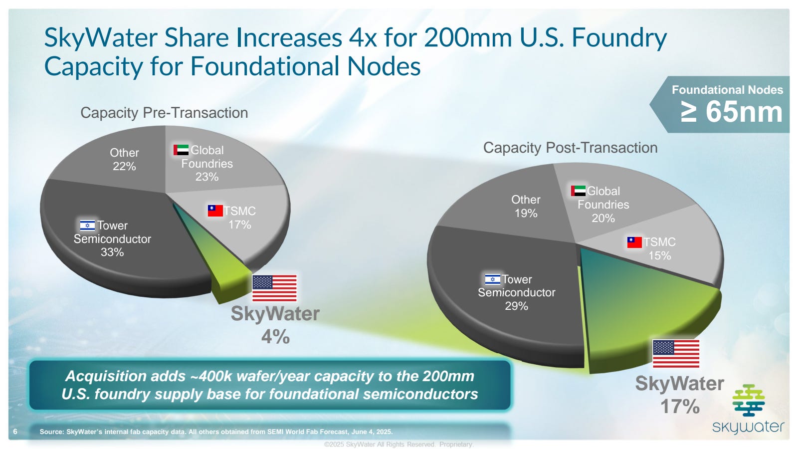
SkyWater Technology, the trusted technology realization partner, today announced that it has completed its acquisition of Infineon Technologies AG’s 200 mm semiconductor fab in Austin, Texas (“Fab 25”). By adding approximately 400,000 wafer starts per year in capacity, Fab 25 brings meaningful scale to SkyWater’s exclusively U.S.-based, pure-play foundry operation and enables SkyWater to enhance its advanced technology services (ATS) offering by incorporating the site’s current capabilities. The facility will play a central role in expanding domestic manufacturing for foundational semiconductor technologies that support embedded processors/MCUs, memory, mixed signal, RF and power applications. In addition, the transaction advances the onshoring of semiconductor production by converting the fab’s capacity from serving a captive integrated device manufacturer (IDM) to operating as a pure-play, open-access semiconductor foundry.
This conversion significantly expands domestic foundry services for a broad base of SkyWater’s industrial, automotive, and defense customers. With the addition of Fab 25, SkyWater becomes the largest exclusively U.S.-based, pure-play foundry service provider offering dual-sourced support for foundational node, 200 mm foundry capacity. Further, SkyWater believes the move directly supports national onshoring and reindustrialization efforts aimed at strengthening the U.S. semiconductor supply chain. SkyWater is one of the only companies actively transforming captive U.S. IDM fabs into open-access infrastructure for secure, high-demand technologies, which is in alignment with U.S. Department of Defense supply chain security mandates.
Here are the details, including a multi-year take-or-pay wafer agreement:
Boom.
TS: We look at Minnesota as our secure manufacturing R&D center. Texas is going to be our high-volume manufacturing center. And then we have Florida as our advanced packaging center. And that combination, gives customers everything they need to not only create new products, but do it in a way where they can have confidence that their ideas originate in the US and will stay in the US, and have a complete value chain to get their products to market.

Chapter 11: America’s Quantum Foundry
Interestingly, Skywater has worked with quantum computing startups since its inception, as mentioned in D-Wave’s 2023 S1 filing:
On December 31, 2012, we entered into an agreement with Cypress for the purchase of available capacity of Cypress’ 8” wafer semiconductor line for the purposes of manufacturing wafers as well as services related to the use of such semiconductor line (the “Semiconductor Line Operation Agreement”). On September 30, 2017, Cypress assigned the Semiconductor Line Operation Agreement to SkyWater Technology Foundry, Inc., to which we consented on November 9, 2017. The Semiconductor Line Operation Agreement, as amended, provides for an initial term of ten years followed by automatic extensions of one year unless either party provides the other party six (6) months prior written notice of its intention to terminate the agreement.
And now Skywater has several additional quantum customers and even bills itself as America’s Quantum Foundry. Interesting!
What’s the upside for Skywater?
What if Quantum takes a long time to pan out?
And what are other risks Skywater still faces?
And other tailwinds?
I’ll cover all that for paid subscribers.