


A 2.3 kW Vera Rubin pulls ~3,286 amps at the die. A Hopper H100 pulled ~1,000. Nearly 11x the conduction loss in three generations! Not good.
Why does the loss compound? Conduction loss in copper scales as I², not linearly. Triple the current, ninefold the loss.
Let’s pencil it out. Vcore (the compute logic supply voltage) is locked at 0.6 to 0.8 V by transistor physics; we’ll use 0.7 V. Given that P = VI, we can estimate the current draw for a few Nvidia GPUs:
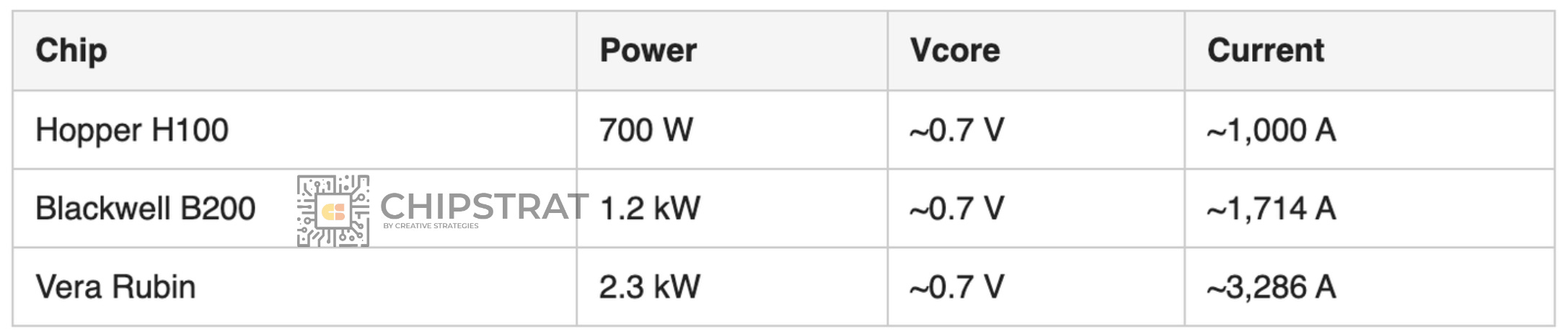
Plug the currents into I². Hopper to Blackwell is ~3x the loss (1,714² / 1,000² = 2.94). Hopper to Vera Rubin is ~11x.
And conduction loss is only half the story. Transient voltage droop, which gets harder as workload transients steepen, adds a second loss term on top.
The only way out is to shorten the high-current portion of the path.
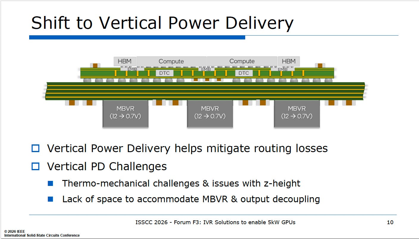
Power delivery is splitting into two domains. The rack-to-board step (48 V to 12 V) stays where it is, because at those higher voltages, the current is still low enough (tens to a few hundred amps) for standard motherboard copper to handle without overheating. The board-to-die step (12 V to ~0.7 V) is where current explodes past 3,000A for a Vera Rubin, and that’s the step that has to migrate from the motherboard onto the package substrate, and eventually under the die itself.
Intel said as much at ISSCC 2026 in February:
Last week, Analog Devices (ADI) agreed to pay $1.5 billion in cash to acquire Empower Semiconductor. Empower ships kilowatt-class power delivery as SiP modules that mount on the package substrate next to the compute die. Short lateral paths, in-package magnetics, but the active silicon still sits beside the SoC rather than embedded inside the substrate. A real step in the right direction, and ADI just paid $1.5 B for it.
Twenty years of IVR attempts have left one architectural step still open beyond Empower: a merchant, on-package, in-substrate, monolithic-magnetics IVR chiplet. A startup called PowerLattice is aiming at exactly that slot.
In this post, we will look at:
How AI accelerators lose power before they compute. The two loss mechanisms worked from first principles.
Intel’s published ISSCC 2026 loss budget for a 5 kW SoC.
Why ADI just paid $1.5 billion, and the impact of Nvidia bumping Vera Rubin from 1.8 kW to 2.3 kW.
For paid subscribers:
What Intel and Empower build today
How PowerLattice’s architecture goes further
Why transient response matters a lot
Which power-IC incumbents lose their AI socket if the architecture lands, which are partially protected, and which benefit either way
What about Nvidia?
How AI Accelerators Lose Power Before They Compute
To keep current manageable, data centers step voltage down in a cascade so the highest-current section is the shortest:
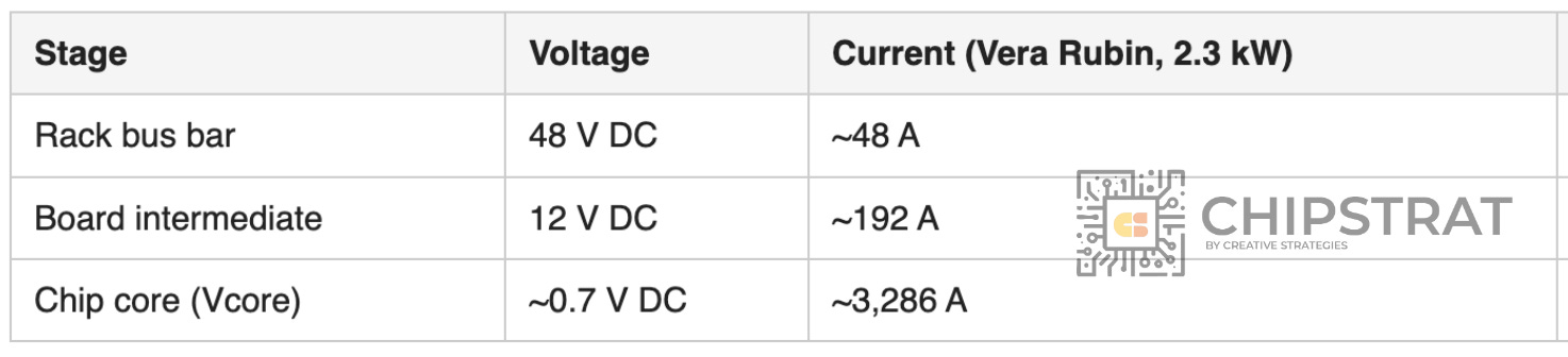
Yikes! That last step, 12 V → 0.7 V at the Motherboard Voltage Regulator (MBVR), has crazy current flowing through it! In current designs, the MBVR sits outside the compute die, either on the PCB just outside the package, or on the package substrate flanking the SoC. Either way, thousands of amps travel horizontally through copper traces to reach the compute die. That lateral path is the Power Delivery Network (PDN), and every millimeter of it loses power two ways:
1) I²R conduction
P = I² × R. Focus on current squared.
Say you have a 200 microohm section of the PDN carrying 1,000 A. That dissipates (1,000)² × 0.0002 = 200 W.
Next generation you roughly triple the current. Same path, same resistance: (3,000)² × 0.0002 = 1,800 W. Nine times the loss!
2) transient voltage droop
AI workloads jump from idle to full power in tens of nanoseconds. The MBVR sits centimeters of high-current lateral copper away from the die. Inductance in that lateral path means voltage at the die sags before the MBVR can respond. If the sag dips below the logic minimum, errors are introduced.
To avoid this, designers add a guard band. So the logic might need 0.75 V, but the MBVR supplies 0.95 V (200 mV of margin):
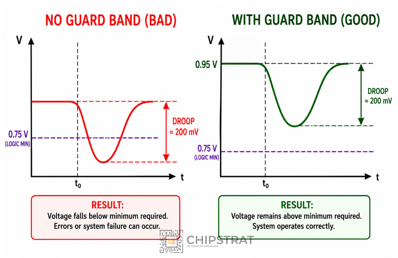
Because dynamic power scales as V², that means we need say ~1.6x dynamic power to avoid droop problems. (0.95² / 0.75² ~ 1.6x)
The ideal fix is move the regulator from centimeters of lateral substrate copper to micrometers of vertical pillar directly under the die.
Putting the IVR (Integrated Voltage Regulator) directly under the load collapses both losses at once. I²R drops because the high-current path shortens by orders of magnitude. Droop drops because proximity allows much smaller, faster inductors and capacitors, so the regulator responds much quicker
Intel’s ISSCC 2026 Chart Puts Numbers on the Problem
At ISSCC 2026 in February, Intel’s Kaladhar Radhakrishnan presented “Integrated Voltage Regulator Solutions to Enable 5 kW GPUs.” Check out this slide that shows the waste that happens to a conventional MBVR architecture as GPU power scales from today toward Intel’s end-of-decade forecast of 5 kW per chip:
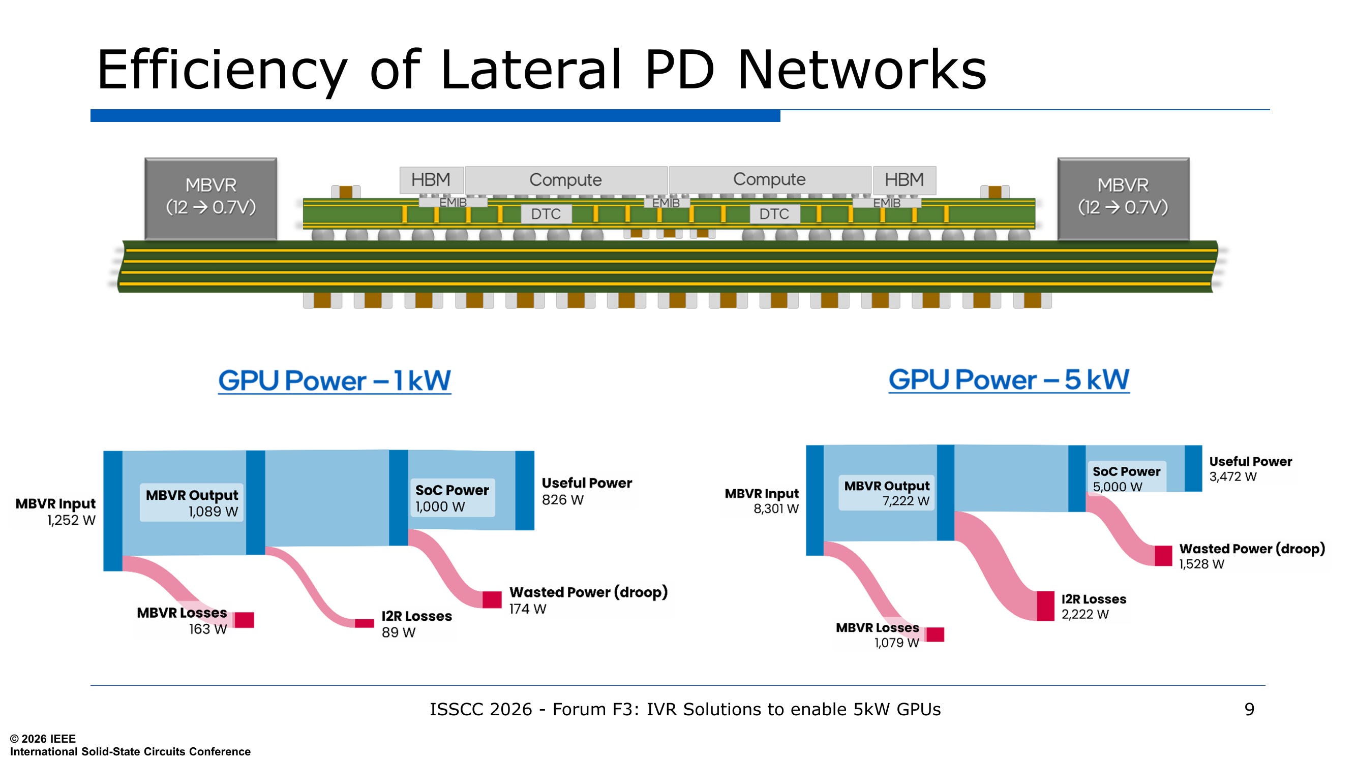
At 1 kW per GPU (Blackwell B200 territory), today’s MBVR architecture is fine. The system draws 1.25 kW from the wall to deliver 826 W of useful compute, for 66% efficiency. I²R loss is 89 W. Droop waste is 174 W.
But at 5 kW per GPU, the architecture struggles. The system now pulls 8.3 kW to deliver just 3.5 kW of useful compute. Efficiency has fallen to 42%. I²R loss has grown from 89 W to 2.2 kW! That’s a 25x jump from only 5x more current, because the loss scales as I².
Droop waste has grown from 174 W to 1.5 kW too.
Roughly half the system input is now burned as heat, not as useful compute.
Intel’s has ideas for alternatives, for example an in-package landside IVR. Landside meaning mounted on the bottom of the package, opposite the compute die, where the BGA balls connect to the PCB.
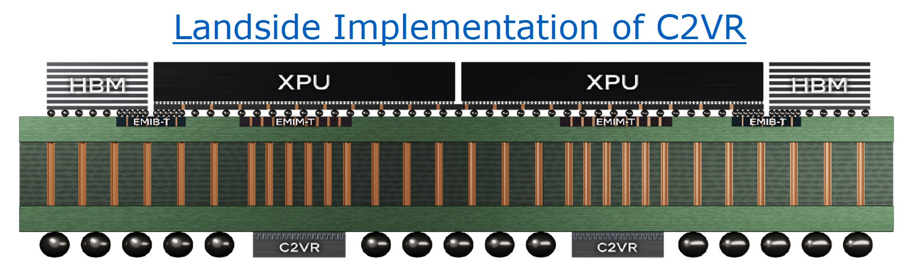
Intel calls one version a C2VR (Continuous Capacitive Voltage Regulator).
Applied to the same 5 kW SoC, the losses are so much smaller:
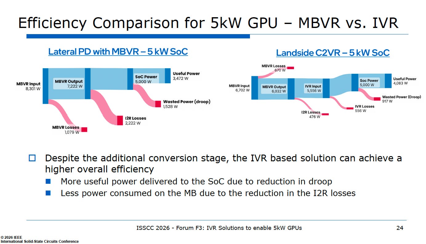
I²R loss on the input path is reduced from 2.2 kW to 476 W. System input falls from 8.3 kW to 6.8 kW. Useful compute rises from 3.5 kW to 4.1 kW.
Same compute job done with 1.5 kW less wall-socket power!
This is a $1.5B problem
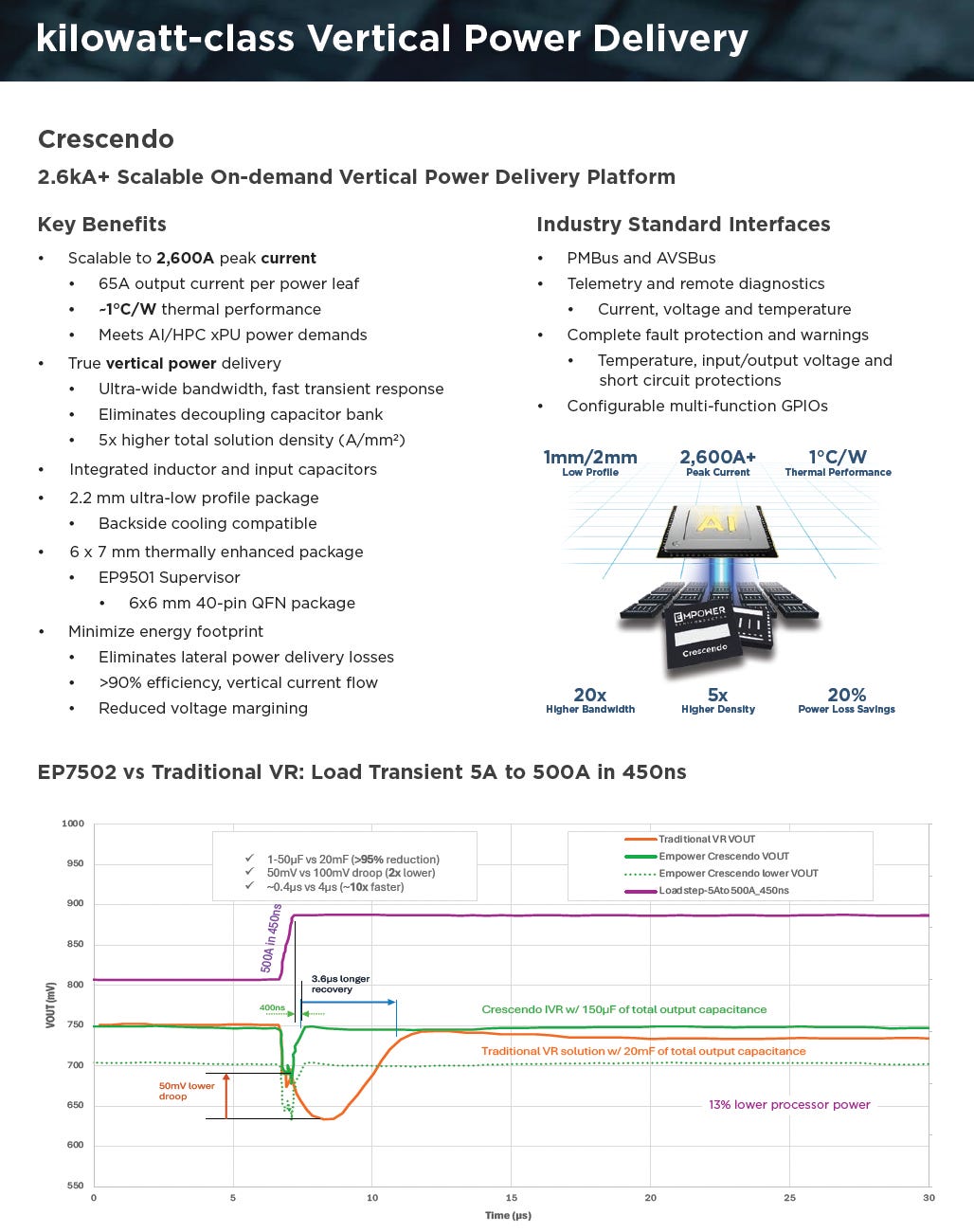
Just last week, ADI announced an all-cash $1.5 billion acquisition of Empower Semiconductor, a maker of silicon capacitors and the Crescendo kilowatt-class vertical power delivery platform. It’s built as System-in-Package (SiP) modules (multiple silicon dies bundled into one package) with integrated magnetics that mount on the package and scale to 2,600 A+ peak current:
My initial take is “Nice! A $1.5B price tag! IVR is an important problem space!”
Of course, Nvidia faces the same problematic physics. Vera Rubin was originally specified at 1.8 kW per chip. In late 2025, SemiAnalysis reported
Supply chain rumors have indicated that there are 2 different “SKUs” with different power and performance profiles: a Max-P variant at 2,300W and a Max-Q variant at 1,800W. However, these are not distinct hardware SKUs but the 2 default power profiles that Nvidia is offering users based on their workload needs. Max-Q is what Nvidia believes offers the best performance per Watt. Max-P offers the greatest absolute performance though this would come with an efficiency penalty. Running the Max-P setting results in a 20% increase in rack power draw but the performance gain fall well short of this 20% power consumption increase.
As we discussed, there are tradeoffs with the 2300W TDP. More watts at fixed Vcore means more amps. More amps mean more I²R and more droop. Which means they really need on-package IVR!
PowerLattice
In November 2025, a startup called PowerLattice emerged from stealth with a $25 million Series A jointly led by Playground Global (where Pat Gelsinger is now a General Partner) and Celesta Capital. The three founders came out of the Qualcomm/NUVIA group.

Peng has a long history of power delivery design, including a 12-year stint at Intel with many patents awarded. Per Pat Gelsinger, it’s a dream team:
“There are very few teams and people that can do it,” said Pat Gelsinger, general partner at Playground Global. “We have assembled what I’d argue is the dream team of power delivery.”
PowerLattice’s innovation is the Rainier micro-IVR, a monolithic, vertical-design silicon die combining proprietary on-die magnetic inductors, advanced control circuits, and a programmable software layer. The chiplet brings voltage regulation from inches away on the motherboard to within hundreds of micrometers of the compute die, eliminating most of the lateral substrate copper that bleeds power to I²R and droop.
The architecture scales by ganging multiple chiplets in parallel, each at a 5 A/mm² current density, with a low-hundreds-of-micrometers z-height. Z-height is thin enough for land-side mounting, substrate embedding, or interposer embedding.
PowerLattice claims >50% reduction in effective compute power, an order-of-magnitude lower power noise, lower cooling, longer processor lifetime, and 2× or more performance per watt where AI compute is data-center-power-constrained.
First chiplets are being produced at TSMC; customer testing planned for H1 2026. Which should be roughly now.
Can PowerLattice compete? What does this mean for ADI+Empower? And other public power-delivery semi companies?
For paid subscribers: Intel and Empower architectures, how the PowerLattice architecture goes beyond, and what it means for publicly traded power-delivery incumbents.