

Intel’s 18A: Misstep or First Step?
RibbonFET, PowerVia, Foundry Roadmap, Potential Write-off, Comparing TSMC

AI, not mobile, now sets the pace for the semiconductor industry. With datacenter power budgets fixed, chip designers must squeeze every watt for maximum performance. Can Intel Foundry rise to this challenge and produce competitive AI chips for external customers?
To answer, we’ll study Intel Foundry’s frontend tech. Is 18A/P a success or a stumble? And what about that Reuters piece?
For paid subscribers, we’ll dive deeper into whether 18A/P and 14A/E offer customers a meaningful alternative to TSMC.
If you're familiar with the technology already or short on time, scroll on down for the juicy bits.
AI Era Context
As imec’s roadmap shows, unlocking the efficiency needed in the AI era means moving beyond FinFET transistors and frontside power delivery. The industry must adopt new gate-all-around transistors (RibbonFET/nanosheet) and backside power delivery.

Intel Foundry is doing just that with RibbonFET, its gate-all-around transistor architecture, and its backside power delivery approach, PowerVia.
Quick Refreshers
We’ll start in the shallow end with a quick refresher. Feel free to skip ahead if you’re already up to speed.
Backside Power: In traditional frontside power delivery, signal and power wires share the same metal layers. By contrast, backside power delivery moves power to the wafer’s backside, freeing the frontside for cleaner signal routing and better performance.

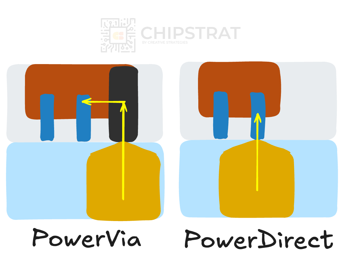
The backside power is delivered to the transistor through tiny through-silicon vias (TSVs):
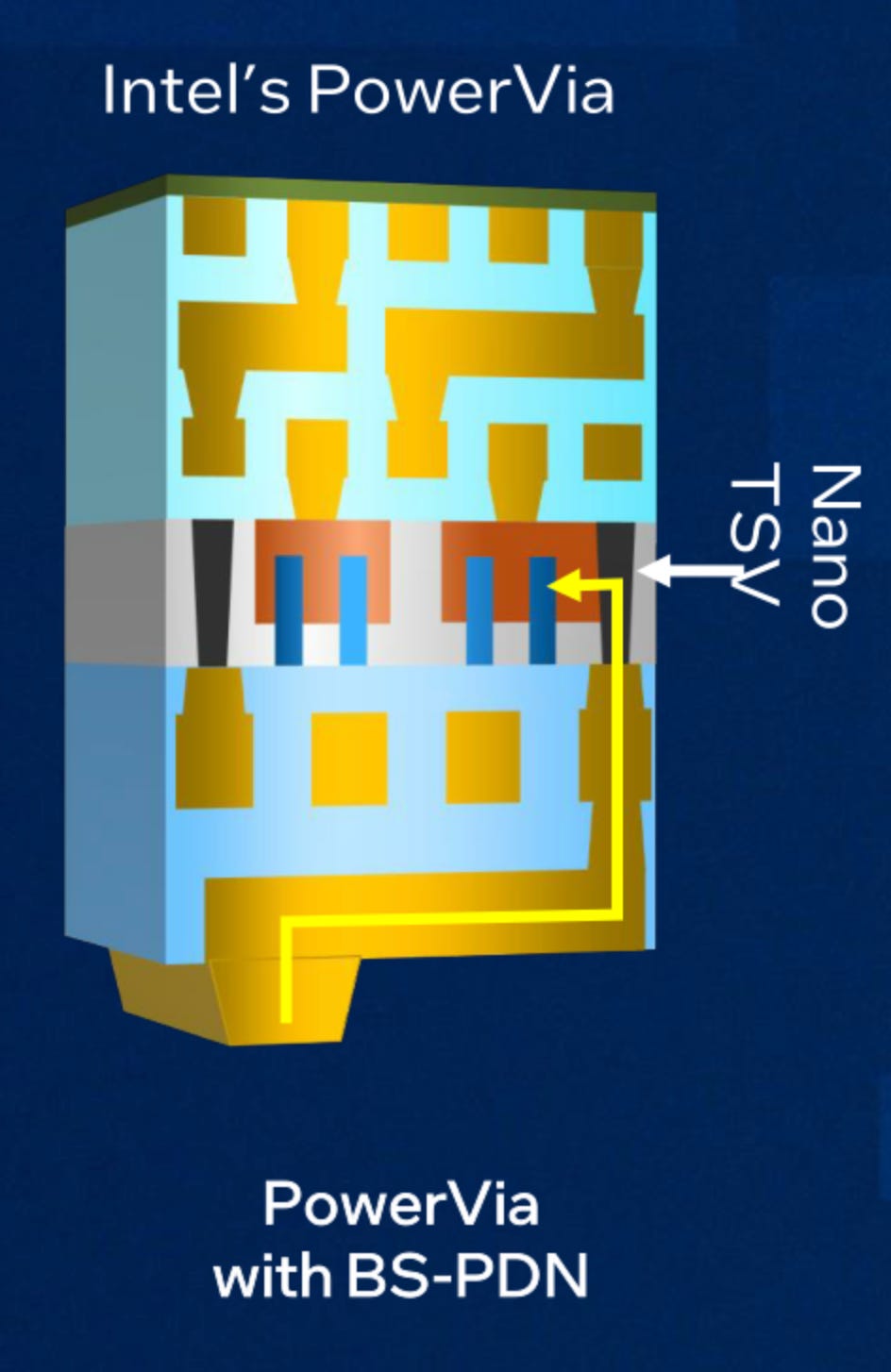
Notice how the power enters from the side of the transistor’s contacts? In the second generation, that power goes directly to the transistor contact. Hence the name PowerDirect.
RibbonFET: Today’s FinFET design uses vertical fins that the gate only partially surrounds, limiting electrostatic control as devices shrink. RibbonFET replaces these fins with horizontally stacked nanosheet ribbons fully wrapped by the gate, an approach known as gate-all-around (GAA):

By fully wrapping the channel, the gate can more precisely control electrostatics, minimizing short-channel effects and leakage even at extremely small nodes. As shown below, RibbonFET delivers significantly higher drive current across a range of voltages compared to FinFET.

Benefits
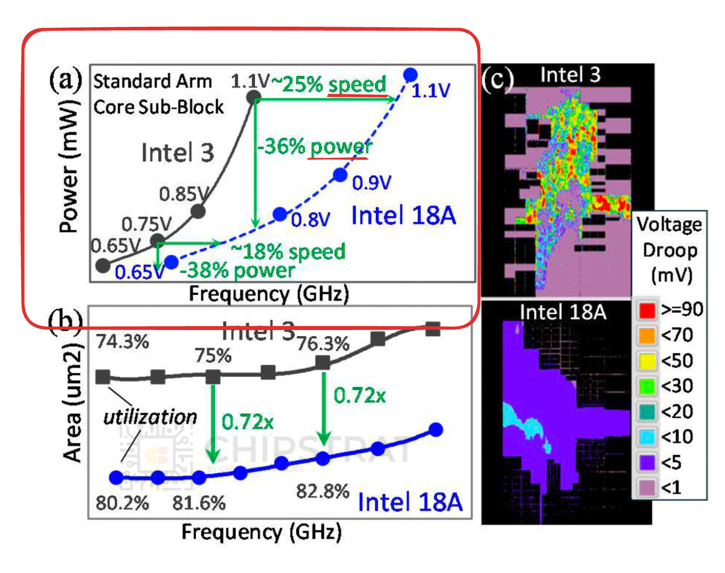
Frontside signals can be wider and better spaced, reducing resistance and capacitance. The resulting RC delay improvements are illustrated in a recent conference paper published by Intel at the 2025 VLSI Symposium in June.

Reducing the RC time constant lets signals travel faster, directly improving timing and frequency.
The paper also illustrates how backside metal (BM) power layers are far thicker than frontside metal (M) layers by one to two orders of magnitude:

Design Flexibility
PowerVia and RibbonFET together let designers balance peak performance and efficiency. XPU designers, for example, could unlock reduced power consumption at the same frequency by lowering the voltage. Other workloads, such as high-performance graphics cards or CPUs, could instead maintain a high voltage to and increase clock frequency.
Higher Density and Standard Cell Utilization
With more frontside area freed up, standard cell utilization rises; designers can pack more logic into the same footprint. More matrix multipliers for your AI accelerator die!

Cost Myth
I was surprised to learn that backside power doesn’t raise costs as much as expected. It sounds complex to manufacture, which usually means higher costs. But simplifying the frontside interconnects helps offset the added complexity on the back.

The Measure of Success for 18A?
OK, so the front-end technology — the combination of RibbonFET and PowerVia — looks promising on paper.
But what do customers think?
Kevin O’Buckley addressed this head-on at Foundry Direct. He made it clear that there’s still work to be done.
KO: 18A is in risk production today and is ramping for our first customers in the second half of this year. Our engagement with customers on 18A – because of the improving maturity of the silicon and all the investments of our EDA ecosystem partners – is resulting in substantial uplift in our platform. We've had over 100 customer ecosystem tapeouts since we started the development technology. It's a technology we really are very proud of.
However, if you reflect back a few years ago when this technology was defined, there was really primarily one voice at the table, a voice describing the primary needs of a company that was developing general-purpose compute processors. We've discovered that work is needed to address their diverse design styles and support more foundry customers in more markets, which is the why behind 18A-P team.
Kevin’s message was clear:
18A was initially shaped for Intel’s internal product needs
But 18A doesn’t meet all the diverse needs of external customers
So 18A-P is a fast-follow derivative
This is believable. Everyone hoped 18A would be a home run and win large external customers, from mobile SoCs to AI accelerators to CPU chiplets. Pat G’s enthusiasm played a role in setting those expectations, even if he didn’t explicitly say 18A would be everything to everyone.
To me, Kevin’s story tracks. When 18A was set in motion years ago, there was no voice representing AI accelerators or mobile. So are we really surprised that adjustments to 18A are needed?
Think about it. While Intel has long built its own silicon, 18A is Foundry’s first process for external customers. (Well, there was a 2013 side project experiment, but that’s apples-to-oranges).
It’s like the first game for an NFL rookie; you’ve played ball before, but not like this! Rookies aren’t expected to dominate their first game. They just need to get on the field, contribute, and learn quickly.
Getting on the field in the semiconductor industry is a familiar theme at Chipstrat. Lisa Su and Mark Papermaster talk about it often when reflecting on their Epyc comeback (for example, here and here).
The first generation shows you’re serious. The second proves you listen and improve quickly. The third is where you shine.
The foundry game is no different. The first external process node needs to demonstrate serious commitment and solid technology. The second node needs to be even better, and still on time. And if you’re doing it right, the third process will shine.
So far, with 18A, Intel is on the field. It took real cultural change just to get in the game. Yet “Five nodes in four years” landed on time and the front-end technology looks strong. Not bad for a rookie.
But what, then, should we make of 18A-P?
18A-P
18A-P adds ribbon width options and extra threshold voltage choices, giving designers greater flexibility to tune PPA for diverse workloads. More than just Intel CPUs…
Yet it retains design rule compatibility, so anyone evaluating 18A can easily kick the tires on 18A-P too.
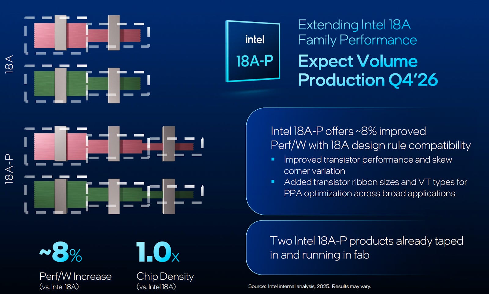
But take note of what this really signals. This is still part of Foundry’s first generation, and it’s not meant to be everything to everyone. It’s a quick, late-stage tweak for teams already exploring 18A.
Reuters
OK. The rookie is now on the field for the first time. The fundamentals are good, and they’re working to get better.
In light of this framing, how should we interpret the Reuters article suggesting Intel may “stop marketing 18A to new clients”?
Here, let me add some emphasis. “Stop marketing to new clients.”
The article sure evoked strong reaction across the industry. Some folks interpreted the article more drastically as closing the door to all external customers. To Reuters credit, they said marketing, not selling. And new clients, not everyone.
But think about it. If you’re a rookie foundry talking to new clients and know your first-generation external process won’t fully meet their needs, why push it? Of course you’ll sell the roadmap and encourage them to try the next iteration.
That shouldn’t be surprising to us at all. It’s a sensible approach.
It’s exactly like Lisa Su in 2017 saying, “Hey hyperscaler, we shipped our first-gen Epyc servers, and the next generation will be even better. I can see the first gen isn’t the right fit for you, but you should give our next attempt a fair shot”.
Hence, the part of the Reuters article about shifting focus to 14A isn’t all that interesting. But the potential write-off they mentioned… that is interesting.
On one hand, a write-off on the first attempt is not unexpected. While painful, it helps clarify strategy for employees, customers, and investors alike. This was the first swing, lessons were learned, now onward. It’s a trade-off; short-term financial pain in exchange for sharper long-term focus and competitiveness.
On the other hand, it could have serious financial consequences. If Intel announces a write-off during its July 24 earnings call, it could weigh heavily on reported earnings, potentially creating a substantial headline impact. The magnitude could be considerable. Remember Rock’s Law… fabs are expensive.
A fab-sized write-off could raise serious investor concerns. Intel will need to position this as a one-time adjustment. It’s the cost of launching a new external foundry business from a standing start.
Remember, this generation of process development (18A) is the culmination of the “five nodes in four years” (5N4Y) initiative, which, in its entirety, should be viewed as an investment in moving down the learning curve.
So can everyone, including the board, remember that 5N4Y was the price of entry? 18A included?
If a write-off happens, it’s important that investors and the board see 18A/P not as a failure, but as the first viable attempt at a long-term roadmap for external customers.
It’s all about framing and expectations.
And — who knows, maybe it’s just a rumor.
Let’s see how the earnings call goes.
14A
If a write-off occurs, it would put a lot of pressure on 14A. But that’s nothing new, right? So how’s 14A, Intel’s next-generation node, looking?
For starters, it’s expected to enter risk production in 2027. Which will make the next 18+ months interesting depending on what we learn in two weeks…

14A introduces second-generation GAA and second-gen backside power delivery, and targets a broader range of customer use cases. As a foundry must!
14A-E is presumably similar to 18A-P: a quick enhancement based on feedback and early customer learnings. We haven’t heard much yet, so that’s my speculation.
PowerDirect
PowerDirect is Intel’s second-generation backside power delivery technology. Unlike PowerVia, which uses nano-TSVs that add resistance and occupy more area, PowerDirect delivers power directly to each transistor contact. This significantly reduces IR drop, so transistors receive nearly the same voltage as at the bump, improving performance per watt. It also requires less area since it eliminates the extra footprint to the side.
So Foundry’s second-gen backside power unlocks more logic from the same footprint and better PPW. That’s the name of the game in AI.
RibbonFET 2
There aren’t many public details yet on the second-generation RibbonFET. But we do know it can be paired with Turbo Cells to give designers even more flexibility. Flexibility for external customers. Again, it seems like Intel is learning…
Turbo Cells
With Turbo Cells, designers can selectively boost performance, for example, only on timing-critical “hot paths”.

Other 14A Benefits
Foundry’s “design once” philosophy continues with 14A. Customers get both PowerDirect and RibbonFET 2 in a single step, rather than having to introduce technologies separately.
Moreover, 14A may introduce High-NA EUV. High-NA enables smaller features while also cutting costs by reducing patterning steps:

Yet Foundry is managing risk by not requiring High-NA for 14A to ship.
Putting it all together
Back in 2021, Intel’s “five nodes in four years” pledge sounded like a moonshot. Yet remarkably, they delivered 18A on schedule, becoming the first to bring gate-all-around (GAA) and backside power to market as planned. It’s not perfect, but it signals that Intel Foundry is serious. They’re on the field — rookies, but playing.
However, shipping a technology is different from shipping products at scale. High-volume production is essential to move down the learning curve and make the Foundry business financially sustainable. Intel Products alone cannot bankroll the external Foundry roadmap indefinitely.
We need to see brand-name customers taping out real SKUs on 14A derivatives. It doesn’t have to be a flagship chip, but it must be more than a demonstration vehicle. This makes 14A business development a critical priority.
The bigger question: can Intel prove it has the financial strength and board support to sustain second- and third-generation external nodes?
Moreover, customers require more than frontend technology. They need robust advanced packaging, strong PDKs, and a mature ecosystem. Will Intel Foundry’s entire second-generation offering (packaging, PDK, etc) work for customers?
After all, no one ever got fired for choosing TSMC.
There’s good news. Foundry does offer differentiation beyond the frontend process we’ve been discussing today.
Differentiation vs TSMC
For paid subscribers, we’ll unpack how Intel Foundry offers fundamentally different value propositions for certain customers compared to TSMC.