


I’ve been thinking about the pros and cons of long-term agreements in the memory market, for both customers and suppliers. As groundwork for explaining the implications, I thought it’d help to build toy supply and demand DRAM models.
Then we can ask whether LTAs change how we model demand, how we think about supply and price, and whether the incentives to bring new capacity online sooner change.
So two overarching questions we’ll look to address
How is today’s memory supply responding to demand, and on what timeline?
Do incentives like LTAs change that in any direction?
This article will begin by building our own simple supply model of the memory market. Not aiming for the best forecast out there, rather a simple enough one to be useful and teach us some important details along the way.
So a basic tutorial to get you started. Teach a man to fish...
Let’s model supply. In subsequent articles we’ll look at demand.
Today we’ll address
Wafer starts and total bits
Cell size and process nodes
Node generations
Node adoption across the industry
HBM impact on bit density
Industry totals
Checking the number two ways
Supply growth model
Node migration puts and takes
HBM wafer absorption
The conventional mix die-size penalty
Capacity coming online
Checking the toy model
Let’s dig in.
One might start with the market-level question “how many bits the industry will produce?”
We can estimate this on a company-by-company basis. If you know the number of wafer starts per month, and the die size, you can figure out how many die per wafer and how many gigabytes of DRAM per die. Then you can make assumptions about yield to get the number of good die per wafer.
bits per wafer = usable wafer area ÷ die area × yield × bits per die
Or more directly, if you have the bit density:
bits per wafer = usable wafer area × bit density × yield
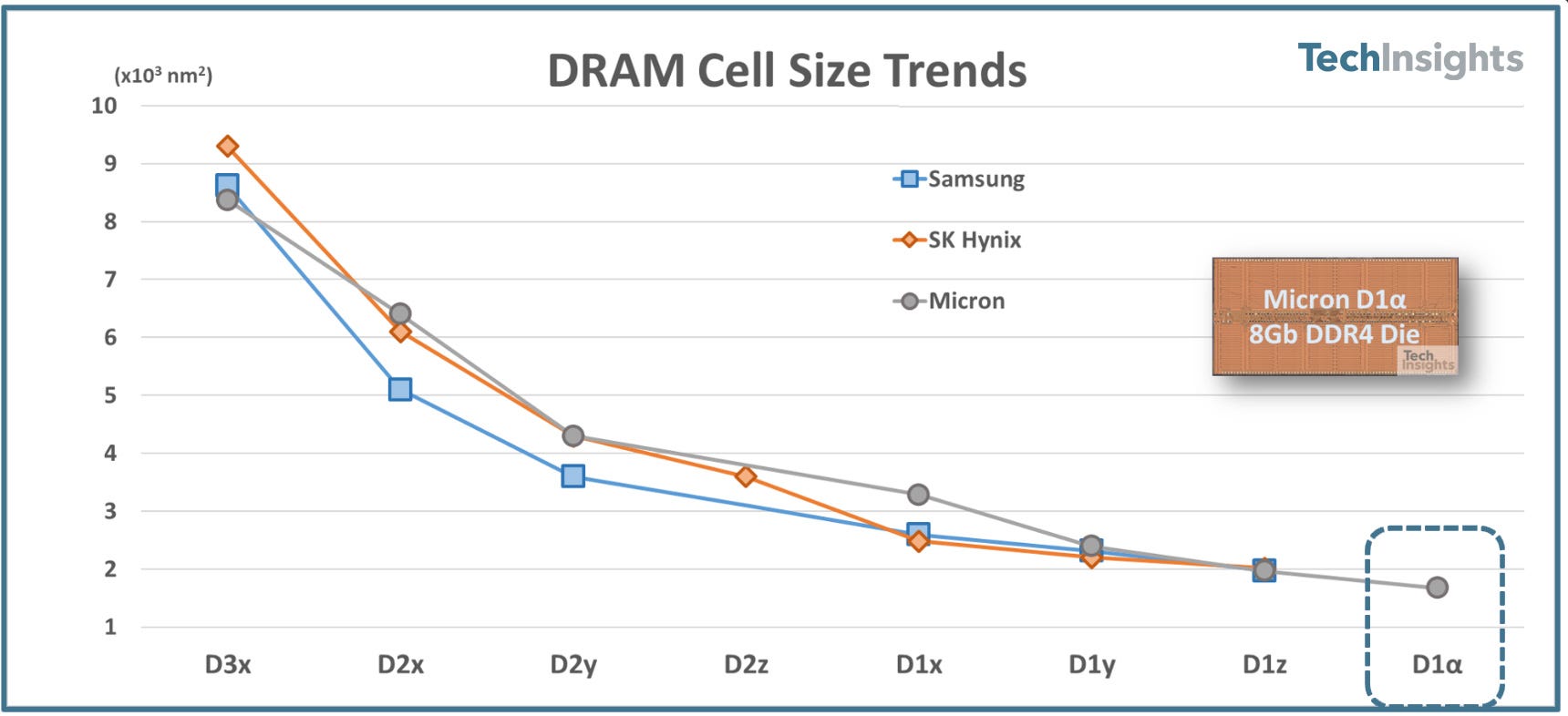
For reference, TechInsights measured Micron’s 1α DRAM at a die size of 25.41 mm² for an 8Gb DDR4 part with a bit density of 0.315 Gb/mm² and a cell size of 1,672 nm².
Plugging that in,
300mm wafer = π × 150² = 70,686 mm²
With a 3mm edge exclusion, and subtracting the partial die that fall off the edge, about 63,800 mm² is usable
63,800 ÷ 25.41 = 2,511 total die
At 85% yield, 2,134 good die
2,134 × 8 Gb ÷ 8 = 2,134 GB, so about 2.1 TB per wafer at 1α
2.1 TB per wafer at the 1α node. Yes, one alpha is actually its name.
Note that not every company can squeeze the same amount of bits out of a given area. It depends on the process node that the company and the fab are on. A DRAM bit consists of one transistor and one capacitor. The area it takes on the die is roughly 6F², where F is the feature size set by the process node.
With each process node, the transistor and capacitor shrink linearly. Because the cell is 6F², the area is reduced by the square of the shrink. i.e., going from say 16.5nm to 11.5nm is a 1.43x reduction in feature size and a 2.06x reduction in cell area. So process shrinks do matter.
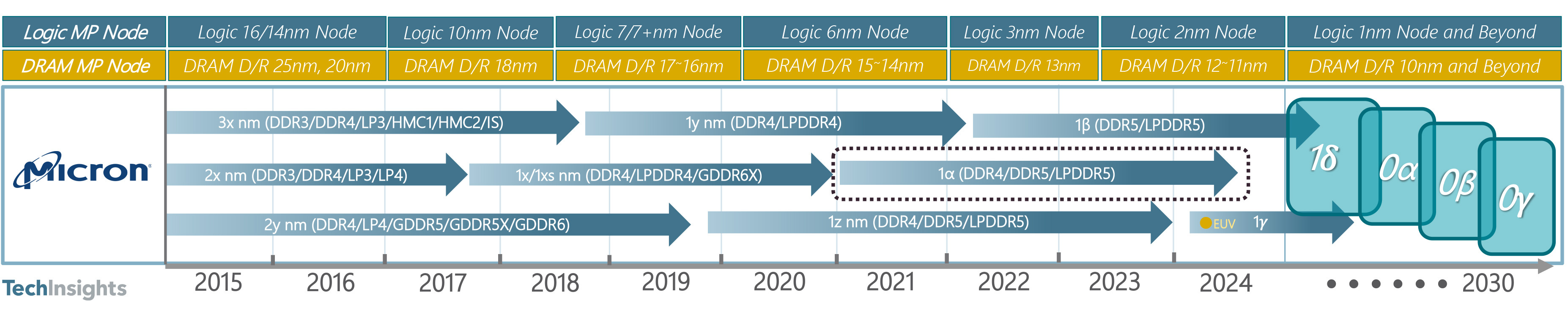
The Greek letters make it obvious that memory process nodes are different than logic nodes. But note that Micron uses Greek letters, while Samsung and SK hynix use Latin letters. Hence 1-gamma and 1c are the same generation. Micron explains why they switched:
“We started with 1x, but as we continued to shrink and name the next nodes, we hit the end of the Roman alphabet. That’s why we switched to the Greek alphabet alpha, beta, gamma and so on.” — Micron
Logic nodes are just marketing today, as there are no transistor dimensions that are actually 2 nanometers or 18 Angstroms. But DRAM generations do somewhat attempt to tie back to an actual dimension, the “half-pitch”.
SK hynix sometimes writes it “1cnm”, “1c-nanometer” and “1c nm”. I don’t know why they include the nanometers bit. The most explicit name is “the sixth-generation of the 10-nanometer technology”.
Here’s the memory process size and naming by generation:
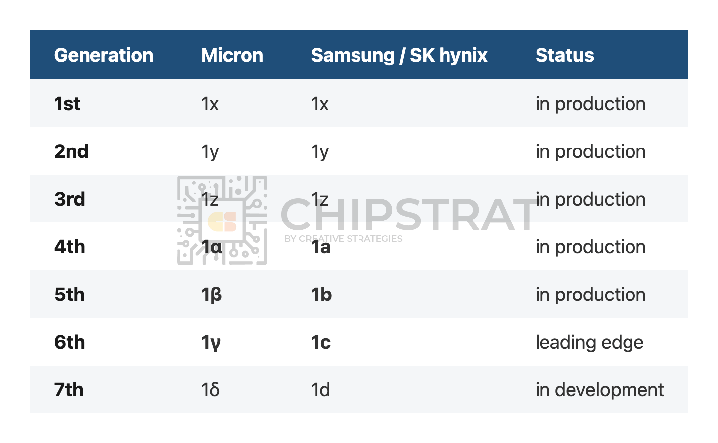
1γ is the leading edge in production, two generations on from the 1α we used in the example above. Bit density is roughly 0.55 Gb/mm², so a wafer capacity is ~3.7 TB. That’s a lot, and is obviously more than the 2.1 TB per wafer we estimated above. So process shrinks matter.
The big three are roughly on the same roadmap, but they don’t get there at the same time. Sort of like TSMC vs Intel vs Samsung Foundry for 18A and 14A logic nodes.
CXMT is behind on process nodes. Nomura’s CXMT initiation puts its mainstream node at 1x-1y, four generations back from the 1γ/1c leading edge. This is an important detail! You can’t just compare wafer starts per month.
Anyway, we’re starting to build some understanding. We can work out the bits on one wafer. 2.1 TB at 1α, 3.7 TB at 1γ.
What else do we need? Well, we aren’t accounting for HBM and how it decreases bits per wafer. Then we need to blend the process mix (not all fabs are on the same process), multiply by each producer’s wafer starts, and compare this total of our bottoms-up approach against industry estimates.
Note that gives us a good understanding of today’s supply, but doesn’t tell us about future supply. And recall we want to understand whether supply can respond to the increase in demand, and how LTAs impact that.
For that, we need to account for growth: what’s getting built, when does it actually produce bits, and any gains/losses from node transitions and HBM mix along the way. All of that is below.
And we have to check all that work and see if we’re on the right track with industry estimates. If not, we should think about why.
Oh yeah, and we’ll pencil out how far CXMT is behind and whether it matters.