

Advanced Packaging: Intel's EMIB vs TSMC's CoWoS
Is Intel's EMIB better than TSMC's CoWoS for AI accelerators? A primer on both, an honest look at the trade-offs, and where it goes from here.

Nvidia’s Rubin Ultra is going to be a huge chip. So huge that it likely takes four reticle-sized compute dies stitched together into one package.

Well... allegedly. There are rumors of a warpage problem on the 4-die package, and chatter that TSMC is leaning on panel-level packaging (CoPoS) to deal with it, maybe even a fallback to a 2+2 config. Hold that thought.
So how do you connect four pieces of silicon together such that they behave electrically like a single chip? That’s the question of advanced packaging. And as AI accelerators keep getting bigger, the packaging itself is becoming the dominant cost variable in the bill of materials.
Today we’ll cover:
A primer on 2.5D advanced packaging, and the reticle limit that started the whole story
TSMC’s CoWoS family (CoWoS-S, CoWoS-R, CoWoS-L)
Intel’s EMIB
EMIB vs CoWoS-L
What is the reticle limit?
The way you make a chip more powerful, historically, has been to make it bigger. More transistors, more compute, more parallelism per die.
The ceiling on “bigger” is the reticle limit: the largest area a lithography stepper can pattern in a single exposure. About 26 mm × 33 mm, or roughly 858 mm².

NVIDIA’s H100 was already pushing the reticle. Blackwell broke through by stitching two reticle-sized compute dies together into a single GPU:

Once you cross that line (i.e. when one die isn’t enough) you need a way to physically connect multiple dies so they behave electrically like a single chip:

That’s advanced packaging. And as accelerator sizes grow, the cost of the packaging itself becomes a dominant economic variable.
What is 2.5D packaging, and why is it called that?

2D is one or more dies sitting directly on the organic substrate. No interposer, no bridge. Routing runs through the substrate itself.
That covers classic monolithic packages and chiplet designs where the dies talk through substrate traces. The constraint is density. Substrate pitch is coarse, so you get moderate die-to-die bandwidth, not the tight compute-to-HBM coupling AI accelerators need.
2.5D adds a passive silicon routing layer between the dies and the substrate. That can be a full silicon interposer, a silicon bridge embedded in the substrate like Intel EMIB, or silicon bridges inside an RDL interposer like TSMC CoWoS-L. It carries fine-pitch routing and sometimes TSVs, but no working transistors. It moves signals, it does not compute.
That is what makes tight compute-to-HBM coupling possible, and it is the dominant architecture in modern AI accelerators.
3D goes vertical. Silicon stacked on silicon — AMD 3D V-Cache, Intel Foveros, TSMC SoIC.
To get nitpicky: 2.5D with CoWoS-S is also technically “silicon on silicon”, but the interposer underneath is passive. Think of 3D as active on active and 2.5D CoWoS-S as active on passive.
HBM stacks are 3D internally, though they usually sit in a 2.5D package.
TSMC’s CoWoS family: three variants
Chip-on-Wafer-on-Substrate (CoWoS) is TSMC’s umbrella for 2.5D packaging. There are three commercially relevant variants. They differ mainly in how much silicon is used for interconnect.
CoWoS-S: full silicon interposer
The original. Entered production with Xilinx’s Virtex-7 2000T FPGA around 2011, where four FPGA slices were stitched together on a passive silicon interposer:

How it works:
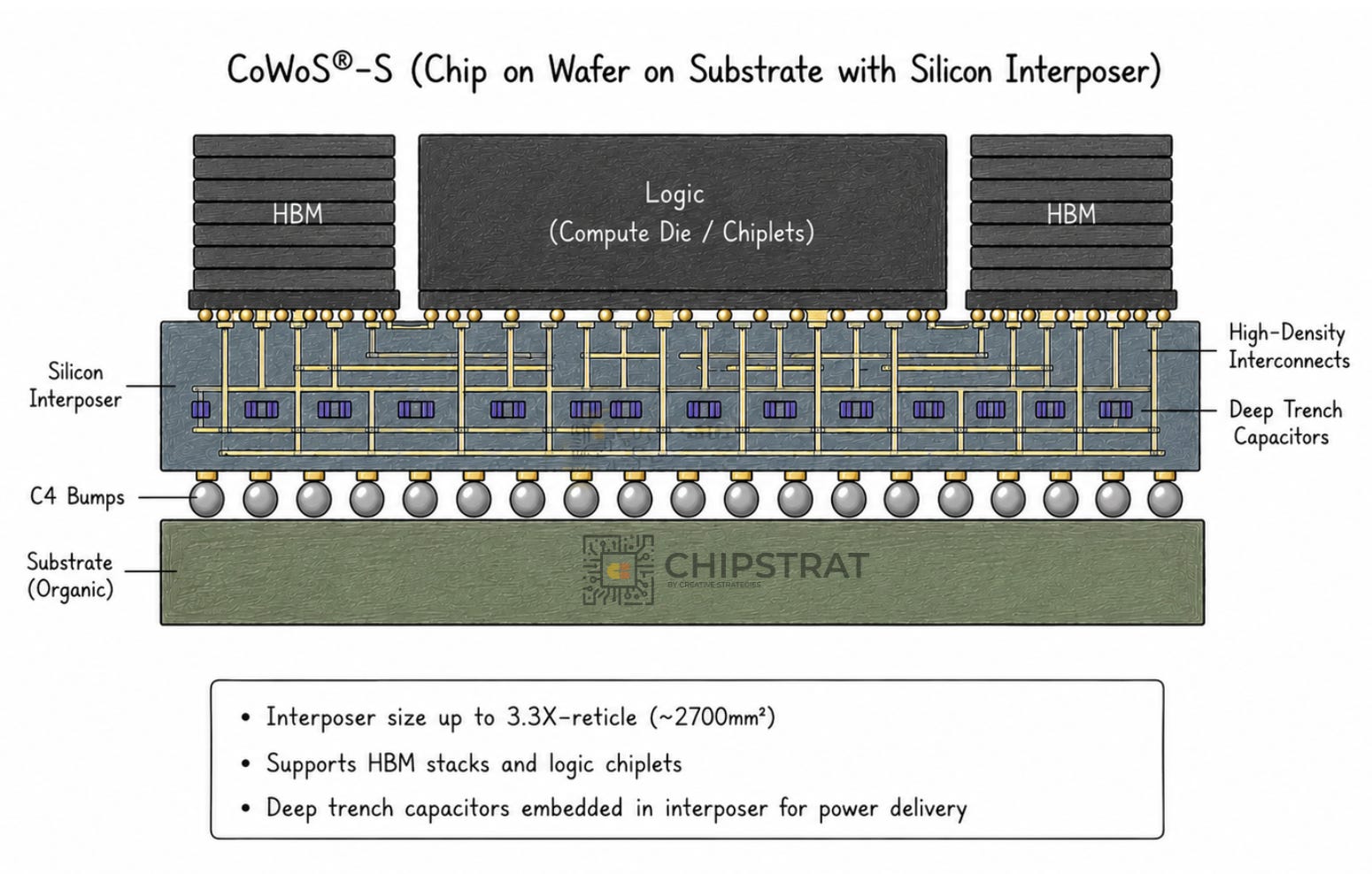
Multiple active dies sit on top of a large passive silicon interposer
The interposer sits on the organic package substrate below
The interposer carries fine-pitch metal routing for dense lateral interconnect, plus Through-Silicon Vias (TSVs) that route signals and power vertically down to the substrate
Important nuance: the interposer is not a “logic chip” in the compute sense. It’s processed on a mature silicon node optimized for routing density and TSV formation, not transistor performance. No logic, no transistors doing work on it.
Think of it as a tiny circuit board made out of silicon. Same job as a PCB, just at lithography pitch instead of PCB pitch, with several fine-pitch metal layers plus a forest of vertical vias.
Electrically, this gives you tens of thousands of short, fine-pitch interconnects between neighboring dies, at far lower latency and power than routing the same signals through an organic substrate.
Here’s what that original Xilinx example looked like:

HBM made this silicon interposer the default approach for flagship AI parts. The HBM interface is too wide and too dense for conventional packaging. Once GPUs adopted HBM (notably AMD’s Fiji / Radeon R9 Fury X), large silicon interposers became standard across every high-end AI accelerator that uses HBM:

There’s an economic problem though. The silicon wafer is being consumed for routing, not compute. That’s expensive. As HBM stack counts grow and compute reticle counts grow, the per-package silicon bill grows right alongside them.
CoWoS-R: organic RDL interposer
TSMC’s response to the silicon interposer cost is to build the routing in Redistribution Layers (RDL) of organic material instead of silicon:

This is cheaper, but isn’t a silver bullet. Organic processes have wider lithographic tolerances than silicon. Trace pitch widens, layer count climbs, and the assembly can’t match the bandwidth density that an HBM-to-GPU interface demands.
Thus, CoWoS-R is useful for cost-sensitive products that don’t need the densest die-to-die interconnect. It cannot carry flagship AI accelerator workloads on its own.
Trade-offs!
CoWoS-L: local silicon bridges in an interposer
TSMC’s current frontier, which places small silicon bridges only where you need high-density routing (compute-to-compute, compute-to-HBM). Use cheaper organic RDL material everywhere else on the interposer.

The bridges sit inside the interposer. The interposer is then attached to the package substrate as one large piece.
This is the TSMC architecture used for Blackwell-class accelerators.
The move is elegant balancing of trade-offs, with silicon where you need bandwidth, organic where you don’t. Beautiful in principle. The catch is that you’ve still got a separate interposer to build (an RDL carrier with those silicon bridges embedded in it), and then you have to dice it and attach the whole thing onto the package substrate. Two pieces, two attach steps.
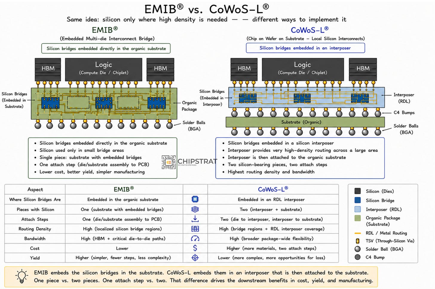
Intel’s EMIB
Embedded Multi-die Interconnect Bridge (EMIB) shares CoWoS-L’s central insight (silicon only where you need it) but resolves it very differently.
EMIB skips the interposer entirely. The silicon bridges are embedded directly into the organic substrate of the package:

Here’s a cleaner version from Intel’s foundry blog:

Note that EMIB has only two layers. Dies and substrate.
EMIB-T and EMIB-M
Worth noting quick: Intel has next-iteration variants. EMIB-T adds Through-Silicon Vias through the embedded bridges themselves, which lets power and high-speed signals flow vertically through the bridge, not just laterally. HBM-heavy designs increasingly need this. EMIB-M integrates MIM (Metal-Insulator-Metal) capacitors into the bridge for on-package power decoupling.
Both are direct descendants of the same “embedded in the substrate” architecture. Worth a watch on Intel’s recent EMIB-T/M explainer:
EMIB vs CoWoS-L, side by side
So EMIB and CoWoS-L are both bridges right? Which is better?
EMIB: silicon bridges embedded directly in the organic substrate. One piece, one attach step.
CoWoS-L: silicon bridges embedded in an RDL interposer; that interposer then attached to the package substrate. Two pieces, two attach steps.
Intel EMIB vs TSMC CoWoS. Update: earlier image had some label errors. Thanks to the reader who caught it!
That one difference leads to these value props:
1. Cost
EMIB doesn’t have a separate interposer to amortize at all. The silicon bridges are small dice embedded in a package substrate that already exists.
Let’s be precise about what’s being compared here. Every flip-chip package, EMIB or CoWoS, sits on a panel-made organic substrate. CoWoS-L additionally builds and attaches a separate interposer (an RDL carrier with small silicon bridges embedded in it) between the dies and that substrate. That extra interposer, plus the extra process steps and the extra attach, is the cost difference. And in current-gen CoWoS-L that interposer is built in round-wafer format, so the panel-vs-wafer waste from the next section applies to it too. EMIB just doesn’t have any of it. The bridges are cheap because they’re tiny, and you get thousands per wafer.
Process steps eliminated:
Interposer build
Interposer dicing
The interposer-to-substrate attach
That’s three places where cost and yield could go wrong, but won’t for EMIB, because they don’t happen.
2. Panel utilization
This is a big one, even if it sounds boring, and it matters more the further along the roadmap we go.
Silicon interposers are cut from 300 mm round wafers. Packages are rectangles. Rectangles on round wafers leave significant edge waste, and the waste fraction grows with interposer size. The bigger the interposer, the more wafer area you throw away at the edges.
Substrates use rectangular panels (a common size is roughly 510 mm × 515 mm). Rectangles tiled into a rectangle. The math is much friendlier.
Intel cites approximately 60% wafer utilization for interposer-class CoWoS versus approximately 90% panel utilization for EMIB:

That’s the cost headline. On a flagship part with a multi-reticle package, you’re looking at a substantial cost-of-goods delta before counting anything else.
And remember the Rubin Ultra rumor from up top? The fix that keeps coming up is CoPoS (Chip-on-Panel-on-Substrate), which is TSMC moving its advanced packaging off round wafers and onto rectangular panels. CoPoS isn’t EMIB. TSMC keeps its carrier-and-RDL approach; it just runs it on a panel. But the package got too big for a round wafer, and the fix is panels. Intel’s package substrate was a rectangle from the start.
3. Scalability past the reticle limit
This one is just geometry.
A reticle is roughly 26 mm × 33 mm = 858 mm².
A 5-reticle complex (think Blackwell-scale, roughly Rubin-ish): ~4,290 mm², or about 43 cm².
A 14-reticle ceiling: ~12,000 mm².
A 300 mm wafer has π × (150 mm)² ≈ 70,686 mm² of total area, and the usable rectangular yield is meaningfully smaller once you account for edge waste and dicing kerf. At 14-reticle interposer sizes, you’re approaching one interposer per wafer.
One. Interposer. Per. Wafer.

At that point the interposer absorbs the entire cost of the wafer. Packaging cost stops scaling and starts cliff-diving in the wrong direction.
EMIB stretches in X and Y across say a 515 mm × 510 mm panel (≈ 263,000 mm² of usable area). The “one interposer per wafer” problem doesn’t arise.
So the cost curves diverge. The larger the package, the wider EMIB’s margin gets.
And packages keep getting larger every generation.
4. Yield through smaller bonded pieces
Bonding a single 5-reticle silicon interposer onto a substrate is a tough operation. You’re moving a ≈ 43 cm² silicon piece through reflow, and silicon and substrate have different coefficients of thermal expansion. Warpage at that size is a yield-limiting problem. Remember that alleged Rubin Ultra issue above?
EMIB attaches dies individually to the substrate. Each attach is small, locally thermally controlled, and decoupled from the others.
Small-piece bonding is inherently higher-yield than big-piece bonding. The yield advantage compounds with package size for the same geometric reason the cost advantage does.
That’s the case for EMIB on the merits. For paid subscribers: three forward scenarios with my thoughts, the “TSMC will just do CoPoS” pushback, the Amkor partnership that adds a second source for EMIB (and why it’s a 2028 story, not a 2026 one), and what it all means for how you read Intel Foundry’s hand. If those tickle your fancy, keep reading.